This thread has been locked.

If you have a related question, please click the "Ask a related question" button in the top right corner. The newly created question will be automatically linked to this question.

OPA828: OPA828 as ADC reference buffer (cap load drive)

Part Number: OPA828

Hi,

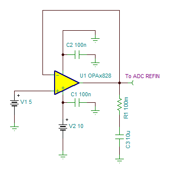
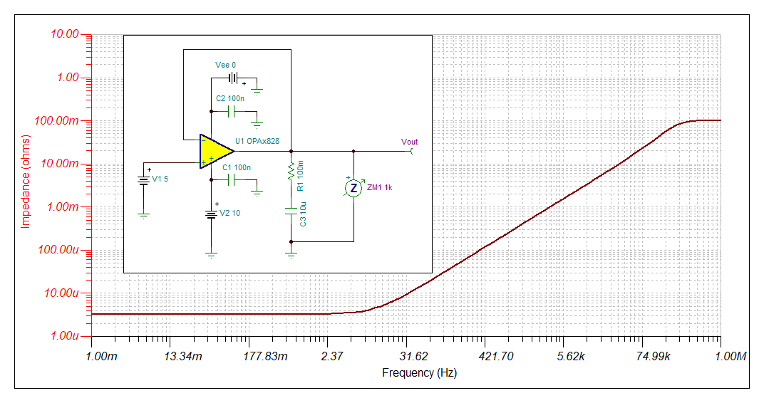
I am considering using OPA828 to buffer a voltage reference for a 15 MSPS SAR ADC, which asks for a 10uF MLCC cap on the reference input pin. I have seen some circuits where the op-amp directly drives the large cap and is stable due to the large value. There are other circuits which use techniques like a series resistor inside the loop with compensation, or an RC snubber. Can the OPA828 be used with a large cap 1-10uF at the output, and if not, which circuit would provide the best performance? Other parts or a composite amplifier would be acceptable too, but OPA828 has a good combination of DC specs and voltage noise.  

Thanks,

Chris

  • Hi Chris,

    From the amplifier stability perspective driving the load, the OPA828 is stable driving a 10uF capacitive load with a small series resistor in the range of 100milliOhms to 220milliOhms as shown below.

    Performing a TINA SPICE simulation (using open-loop stability analysis) and plotting the loop gain of the circuit shows the phase margin of the circuit is ~60 degrees while driving a 100milliOhm+10uF load. 

    The transient response/settling of the OPA828 reference driver circuit is dependent on the dynamic switching load of the SAR ADC. Therefore, the SAR ADC reference input dynamic/switching load needs to be modeled to ensure the circuit is able to support the max sampling  SAR ADC rate required in the application, and to verify that the reference voltage remains settled between SAR ADC conversions (and ADC conversion clock cycles).  If you need us to look into this detail, please provide a SAR reference input equivalent model for the ADC (or let us know which SAR ADC device is driven).

    Thank you and Regards,

    Luis 

  • Thank you for taking the time to check that! 

    The ADC is the LTC2387-16, the equivalent circuit for the input is:

  • Hi Chris,

    The ADC datasheet suggests using an LTC6655 as a possible ext reference while overriding the internal ref buffer of the ADC. This reference device has higher output impedance over frequency than the OPA828 buffer circuit; therefore, based on the output impedance over frequency response of the OPA828, the OPA828 buffer with the 100mOhm+10uF load will drive the ADC REFBUF pin without issue. 

    Since the output impedance over frequency of the OPA828 buffer+10uF is much lower than the suggested external reference with the 10uF load, the OPA828 is able to recharge the switch capacitive load of the ADC and settle faster, and therefore the OPA828 reference buffer circuit is optimal driving this ADC.

    Please see below the TINA simulation of the closed-loop output impedance of the OPA828 with a load of 10uF+100mOhm. 

    Thank you and Best Regards,

    Luis

  • Hi Chris,

    Corrected the simulation image below, to show the output impedance plot over frequency including the 10uF and 100millOhm load.

    Thank you and Regards,

    Luis