This thread has been locked.
If you have a related question, please click the "Ask a related question" button in the top right corner. The newly created question will be automatically linked to this question.
Hello,
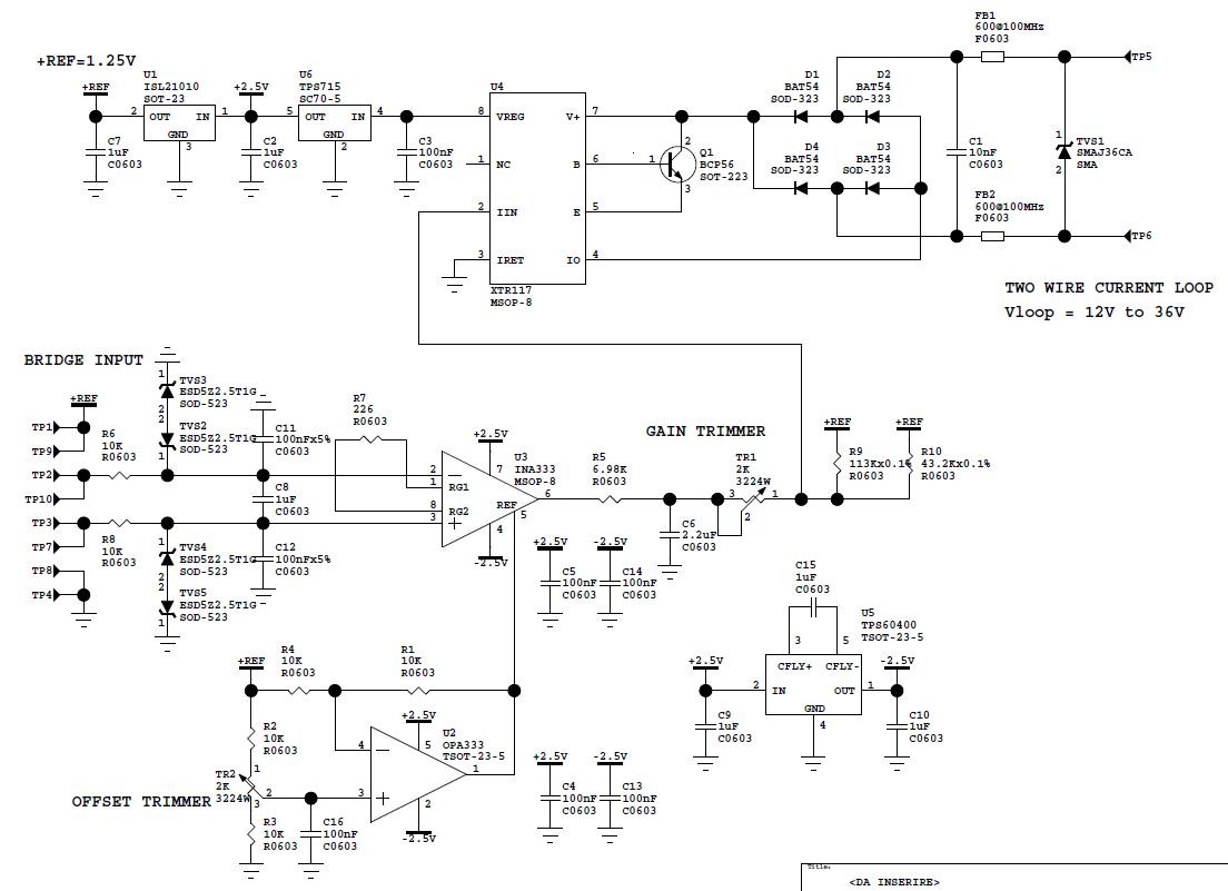
I am trying to generate a -2.5V supply from XTR117's VREG pin. I am using a TPS71525 with a fixed 2.5V output to generate a +2.5V from VREG pin. After then I used a TPS60400 (charge pump voltage converter) with 1uF capacitors (Cin, Cout an Cfly) to get a -2.5V, but the circuit is not working. There's no other load other than the circuit a have described. I misured the voltage on XTR117 VREG pin and I get a value of 1.27V. It looks like that TPS60400 represents a heavy load for the regulator inside XTR117, but the typical quiescent current of TPS60400 is only 65uA.
Following schematic of related section.
What should be the problem ?
Can somebody help me please?
Thanks in advance.
Amauri
HI Amareuli,
1) Is IRET floating with respect to the loop GND? The XTR117 is a two-wire transmitter and IRET must not be connected to the 4mA-20mA loop ground. Please confirm if IRET (local XTR117 IRET node on your schematic) is allowed to float with respect to the external loop supply GND. All the driver circuitry needs to be referred to IRET (as shown on your schematic), but you need to ensure IRET is allowed to float with respect to the external loop supply GND. The blog below discusses issues with shorting IRET with the loop supply GND...
2) The XTR117 is a two wire 4-20mA transmitter, and the total current consumption of the complete two-wire transmitter circuit (XTR117+all other circuits) must be less than <4mA. The post above mentions that there is no other load, but which circuit are you planning to power-up with the +2.5-V and -2.5V supplies? Your schematic does not show the circuit that will be powered by the -2.5V.
For a more detailed explanation, please see blog below.
2-Wire 4-20mA Sensor Transmitters: Sensor and Transmitter Current Consumption Limitations (Part 3)
3) What is the voltage of the loop supply?
Thank you and Regards,
Luis
HI Luis,
Thanks for the answer.
1) I confirm that IRET is floating and isolated from current loop side. All circuitry on signal conditioning side is referred to the local GND.
2) The signal conditioning circuitry is made of a INA333 (instrumentation amplifier) and a OPA333 that provide the VREF signal for the INA333. I want to amplify the signal from the bridge and compensate for some positive or negative offset to get a zero volt at INA333 output pin when my input signal is offset. Doing so I can use two independent trimmers to set gain and offset for my signal, that is I can calibrate offset trimmer without having to recalibrate gain trimmer and vice-versa. That is why I chose to use a double supply (positive and negative) to power the circuit. I can confirm that consumption is less than 3.7 mA.
3) For debugging I am using about 15V volts for loop voltage.
Now I added the complete circuit schematics.
Any idea, suggestion or consideration about the circuit will be very appreciated.
Thanks you again and best regards,
Amauri
HI Amauri,
One suggestion you may try to debug, is to add a couple of ~ 2.7V TVS or Zener diodes at the +2.5V and -2.5V supplies (referred to IRET) as shown below.
On this circuit, the positive +2.5V power supply will turn on prior the charge pump -2.5V negative supply, and the negative supply may be high impedance or float at start-up. Therefore, the circuit current may flow on unpredictable, parasitic current paths at start up; potentially causing issues at start-up where the amplifiers are not properly biased.
When using the TVS/Zener diodes, ZS2 will forward bias at power up, preventing the negative supply to float, ensuring that the negative supply is held close to the IRET potential, and is held more negative than the +2.5V supply, providing a path for the OPA333/INA333 quiescent current to flow until the negative charge pump power supply turns on.
See below.
It appears the bridge sensor is biased between VREF=+1.25V and IRET, where the bridge will produce a signal that has a common-mode of ~0.625 above IRET. Do you still need the negative -2.5V supply? What is the full-scale voltage expected from the sensor?
Thank you and Regards,
Luis
Hi Luis,
Thanks for you suggestion about the zener/TVS. It's correct. I will take it in account on the new design.
But the prototype I am debuging has only assembled the components you see in first schematic I posted. I have yet trouble with power supply in that situation. That's the reason I said before I have no other loads on power supply. I did it to reduce the area to search for the trouble.
I don't know why but this circuit seems to be biased not correctly on start-up. The TPS60400 doesn't start and doing so it looks like a heavy load for VREG pin from XTR117 reducing the voltage on this pin about to 1.27V and again below the minimum voltage the TPS60400 needs to start-up.
I made an experiment: I disconected the pin 2 of TPS60400 (IN) from the +2.5V supply. I powered up the prototype and I got the VREG and +2.5V working correctly. With the prototype still powered up I connect back the pin 2 of TPS60400 to the +2.5V supply and it began to working correctly generating the -2.5V voltage. I need help to understand this issue.
I need the dual supply because the bridge can have small offset voltage (positive and negative) that I have to eliminate to get a zero volt on the INA333 output. Doing so this offset that is near zero volt will not be amplified making the gain setting indepent from offset setting. This is a specific request for this project. To achive this I need to be able to generate a positive or negative voltage on VREF pin of INA333. That's reason I need both positive and negative power supply.
Otherwise using only positive supply I don't know how to get same solution.
In any case I would like to focus also on the problem related to the dual power supply described above.
I hope to be clear this time in describing the my problem.
Many thanks again.
Best regards,
Amauri
Hi Amauri,
In the past, while working on a different system solution, involving a DC-DC converter on an application where the input supply current was very limited, I had issues on start-up due to the in-rush current required by a DC-DC converter at start-up. The in-rush current required by that DC-DC converter at start-up was higher than the expected current consumption once the device was powered up. On that particular case, I was able to work around the problem by powering the supply in stages, and also controlling the ramp-up rate of the DC-DC converter. In that particular design, I used the enable pin of an LDO regulator with a voltage divider and RC filter to create a delay.
Since in your experiment, the TPS60400 supply works well once the XTR117 regulator is powered-up, one possible solution is to add a delay on the +2.5V/-2.5V supply.
One possibility is to modify the design using a +2.5-V LDO that incorporates an enable pin, with a similar circuit as shown below. This would allow for the XTR117 regulator voltage to completely ramp-up first, where the bypass capacitor at the XTR117 regulator will be fully charged to 5-V first, harvesting enough energy to power up the rest of the supplies, and after a ~10s -100s of millisecond delay, the RC filter on the LDO enable pin will charge up to the require threshold, and power-up the +2.5V LDO and -2.5V charge pump. The voltage divider values and capacitor value on the enable pin have to be designed to ensure that the enable pin always reaches the minimum required threshold of the enable pin after a desired delay. Below is a link to an application note discuss this topic. Also, below there is an example of a regulator with voltage divider and capacitor on the enable to create a delay. Alternatively, you could also consider using a watchdog timer device to program a delay on the enable pin of the LDO. Please also ensure to use the TVS diodes (or zener) on the +/-2.5V supplies as previously discussed.
http://www.ti.com/lit/an/slyt730/slyt730.pdf
The Power Management application engineers may have good suggestions for LDOs or power supplies to be used on your XTR117 design. Consider submitting a query on the forum below.
https://e2e.ti.com/support/power-management/
Thank you and Regards,
Luis
Hi Luis,
Today I was thinking to do exactly what you are suggesting me now, that is, power up the vary stages in sequence using a delay between them. I was not sure that will give me a good result but when I just hear from you about your past experiences with similiar circuits I began to believe this suggestion will solve my problem. In fact I already have got a voltage regulator with an enable pin to make this test. The result was positive. The circuit is working perfectly. Now I have only to optimize the value of RC circuit to get the minor delay.
Many, many, many thanks Luis.
Best regards,
Amauri