This thread has been locked.

If you have a related question, please click the "Ask a related question" button in the top right corner. The newly created question will be automatically linked to this question.

THS4521: Pspice Model Issue, INTERNAL ERROR -- Overflow, Multiply

Part Number: THS4521
Other Parts Discussed in Thread: THS4121, THS4130, THS4551, , TMS320F28379D, LM7705, THS4531A, AMC1311, THS4531

Hi

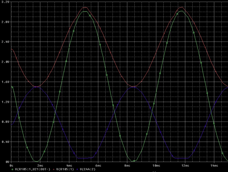
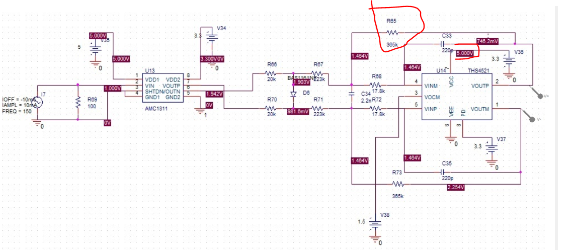
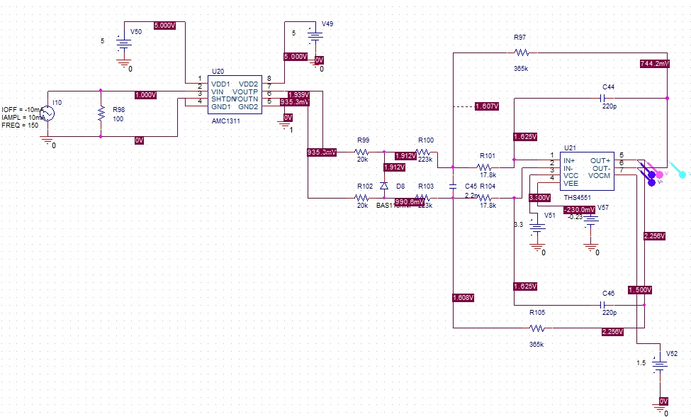
When triyng to simulate the Pspice model the folowing message appears:

What causes this? I think that all the parameters are ok. I tested the same filter topology with other OPAmps (THS4130, and THS4121) with good results.

Thanks in advance

Carlos Alonso

  • Hello Carlos,

          I am unable to view the image/file. You can use the insert file or insert/edit media icon within the reply window. Follow this post to correctly insert a file or image: https://e2e.ti.com/support/site-support/f/1024/t/761613.

    Thank you,

    Sima

  • Sorry, first time posting.

  • Before you get too far here, keep in mind the THS4521 was 1st gen on this type of part, the THS4551 upgrade fixed a lot of issues on that part and is far superior in noise and HD.Also, much better model - 

  • Thanks for the reply.

    I didn`t use the THS4551 because there is no Pspice model in the web. But searching a little bit more I found a thread that solve this problem. I didn`t know that it was so simple to convert from Tina Ti to Pspice. I have tried with other models without success..

    https://e2e.ti.com/support/amplifiers/f/14/t/870945

    Now the problem is that the differential output seems to be ok despite the negative output does not reach zero... 

    Our goal is to find a differential amplifier supplied to 3V3 or 5V that interfaces with the TMS320F28379D ADC with a range of 0 to 3V (0-2V input, G=1.5 , Vcom=1.5V) for a possition sensor measuring (sin/cos signals 0-20 mA and 100ohm sensing resistor)

    We have tried with the THS4121, 4531, 4505, 4131 without success.

    After simulating this one, the best aproach is the THS4551. But we continue needing to reduce the gain to avoid the lower limit as sown in the image above.

    We where using the THS4130, but we want to avoid that if for some error the Operational goes to -5V it does not damage the DSP.

    Could you recomend other amplifier family? 

    Perhaps I should move this question to another thread?

    Thanks in advance

  • Yes Carlos swinging to ground on a single supply design is not possible - we often recommend the LM7705 negative 0.23V generator to power the negative supply to get the required headroom, 

    This comes up so often, it was covered in the 1st couple of this article series I am doing, 

    https://www.planetanalog.com/input-and-output-voltage-range-issues-for-high-speed-cfas-and-fdas-insight-2/

  • Thats really helppuful! Thanks!

    But we really don need the full scale of the differential output as the input signal from the sensor goes from 4-20 mA. So on the sensing resistor we have 0.4V and after the Operational 0.6V. This margin is used to detect that there is no signal on the line. The usefull range is 0.6-3V.

    We could deal with some distorsion near zero. But what I don't understand is why if the inverting oputput does not reach 0, the differential signal reaches 3V. How is this possible?

  • can you insert your TINA file?

  • It is Pspice

    I used the file from the thread I found and that I mentioned above.

    I mean this:

    The non-inverting output supplies the part of the signal that need the differential to reach 3V. But I don't know why and what effects could it have on the ADC meassure

    Both simulations are with the THS4551 with the Pspice model obtained from Tina TI file and the schematic form my first post.

  • Ok, so you are not using TINA, fine, looking closer at your first circuit - this is an MFB filter using R values that way too high for this fast a part. Drilling down layer by layer is much easier in sim, but just as 2 observations - 

    1. R values this large might be introducing a large output DC offset through the Ios term in model, 

    2. it looks like a 3.3V supply? yet the probe seems to show 5V? 

    Perhaps someone in the product group could duplicate this circuit in TINA to go further. Also, I have considerable MFB design tools, I could extract your target, but if you could just tell me what you are trying to do, I can quickly send you some better RC values (from a noise, stability, etc standpoint). 

  • Thank you so much.

    1- The R values are calculated through the filter equations to obtain G=1.5, fc= 2kHz and Q=0.88

    2- The schematic is from the part THS4521 that does not working. This was the first issue of the thread. I don't know why pspice gave me that values. But I tried wit both supplies, 3V3 and 5V with the same error.

    This is the actual design with the THS5451

    The objetive is to obtain differential signals from a position sensor (sin, cos) for a motor drive. The max freq of the signals is 150 Hz, so we put the cut-off freq at lest 1 decade above, at 2kHz. 

  • Here is your filter updated to better values, same shape I think assuming that 2kHz you mentioned was Fo and F-3dB. Here is the file for product group folks to pursue further, 

    THS4551 2kHz MFB.TSC

    1. I changed your protection diodes to BAV99 (you usually need both polarities, 

    2. I set the Vocm to 1.65V but 1.5V should work also

    3, Post RC is set to zero now, usually there is something there, add it if you have it

    4. Inside the loop R's isolate the open loop Zo from the feedback C - very useful for improving phase margin - you can take those out for now if you layout is done, but if not leave a place for them. I think those showed up in this article, and why - 

    https://www.planetanalog.com/stability-issues-and-resolutions-for-high-speed-fully-differential-amplifiers-fdas-insight-8/

    5. The THS4551 is pretty fast for this app, the other part to consider is the THS4531A. 

  • Thank you so much!

    Those R values are much more better. But how do you obtain them? Using the equations that I commented the values are really different.

    Any way we tested with your values and adjust them to obtain exactly 1.5G. We also add the 20ohm Rs and this is our result with the THS4531A

    1- The Diode we used is not a protection diode. We use it due to the FailSafe mode of the AMC1311. When the input power supply fails the output goes to -2.6V. If this enters the THS x1.5 the output saturates at -3V3 and the ADC meassure range in differential is -Vref/Veref, this is -3/3V. Putting the diode to work in this way the input to the THS is the voltage drop on the diode and the input to the ADC is meassurable. We choose the BAS116 due to is low leackage current that could impact in the meassure when it is in inverse. 

    2- We set Vocm to 1.5 as it is Vref/2 ot the ADC

    3- We did not add yet de RC ouput. We shall cacultate the values to fit with the ADC sampling freq.

    4- As sujested we add the 20 ohm R inside the loop and we will study your article.

    5- The previous simulations are with the THS4531A and seems to fit well!

    Again than you so much!

  • You are welcome Carlos, 

    well the RC values are a long story. Essentially 

    1. The academic material simplifies for teaching purposes by going equal C or equal R to reduce degrees of freedom - that leaves untapped dynamic range on the table. 

    2. You can constrain your solution more reasonably in several ways - one is to scale the R's to not significantly increase the noise over the op amp only noise, 2nd is to limit the C0G C selections to E24 and max values less than where they get prohibitively expensive (I have that at 33nF right now occasionally checking pricing),  3rd is to set C ratios to reduce internal noise gain peaking

    3. Then you can adjust the RC's for op amp GBP using  a cubic transfer function and iteration

    I kind of got into this area in this original app note

    http://www.ti.com/lit/an/sboa114/sboa114.pdf

    that had an error in the cubic coefficients that I later corrected in a Planet analog article - 

    https://www.planetanalog.com/include-the-op-amp-gain-bandwidth-product-in-the-rauch-low-pass-active-filter-performance-equations/

    I took this material quite a bit further in building the Intersil online filter tool  back in the 2009 to 2013 time period (and the SKF flows as well)

    At the time I published a lot of those solution flows on EnGenius AnalogZone that have since disappeared. 

    But, this left me with an increasingly sophisticated design spreadsheet to spin these out pretty quickly with a parametric amplifier database spanning over 250 devices. It is important to have good parameters for these designs that include 

    1. Correct GBP - a lot of tools have the wrong numbers from poor datasheets, discussed here - 

    https://www.planetanalog.com/why-is-amplifier-gbp-so-confusing-insight-12/

    2. Also important to have something more than a guess on required minimum GBP margin, discussed here, 

    https://www.planetanalog.com/use-true-gain-bandwidth-product-to-estimate-required-margin-in-active-filters-insight-13/

    3. parasitic input C that becomes part of the cubic design coefficients - oddly that does not increase the order to include that but it does change the solutions

    4. Amplifier noise terms to use in scaling the R's (the other constraint there is on the min input R that acts as a load to the prior stage - very important in multistage filters. You can always improve noise going really low on the R values, but if the prior stage can't drive it you can't hit the desired shape). 

    Glad those worked out for you - I could rerun the RC's using the THS4531 parameters but you have it working now - oh well, it is pretty easy - it came out the same, stick with those. 

  • Oh incidentally Carlos, I noticed you commented on the gain adjustment you made - more detail is needed, 

    So the other step I added not long ago was to test closeness of fit to standard E96 R values around the exact R solutions having selected standard e24 C values - here is that step for your design showing the 8 permutations and fit error to target, This is focused on best Fo and Q fit where I assume gain mismatch to target can be made up somewhere in the chain. Your choice - the values I gave you have the lowest Fo and Q fit error, but probably not too critical in your app. The gain in this nomenclature is R1/R3. So actually looking at these row 6 is pretty good with almost exact gain match - might use those if you have not already. 

  • It is true that the Gain mismatch could be corrected on the ADC, but we decided also to unify components.

    With these values we obtained the results from above and the thoretical values do not differ too much:

    R1= R2 = 6.98k

    R3= 4.65k --> 1k + 3.65k

    Your solution          K= 1.4645 ; Q = 0.8813 ; fc= 1.996 kHz

    Our New approach k= 1.5011 ; Q = 0.8678 ; fc = 1.9243 kHz