This thread has been locked.

If you have a related question, please click the "Ask a related question" button in the top right corner. The newly created question will be automatically linked to this question.

OPA551: OPA551 parallel connection

Part Number: OPA551

Hi team,

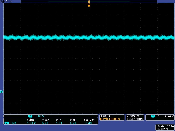
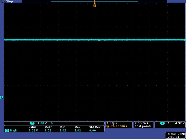
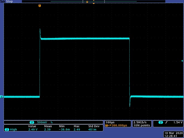
I am trying to use OPA551 with a voltage follower (gain = 1). I am trying to increase the output current by using a circuit configuration that uses two operational amplifiers described in Fig. 29 on page 14 of the data sheet. However, if I check it with an experimental circuit, the output will appear to oscillate. Do I need any additional components for use with voltage followers? In the experimental circuit, there is no R1, R2 = 0ohm, RS = 20ohm. No output load (RL) is connected.

Best Regards,
Tom Liu

  • Hi Tom,

    I need more information from  you. I simulated the circuit with the limited information you provided, I am getting inconclusive simulated results. Please send us the following data. 

    1. Send us a schematic.

    2. Please place a 1kOhm or actual load at the output of the op amps. 

    3. which frequency are you starting to see oscillation? Are you doing doing step function or sinusoidal at input?

    4. Single rail  or dual rail etc.

    Best,

    Raymond

  • Dear Raymond,

    I am the original questioner and provide the required information as follows:

    1.Rough schematic is attached below.

    2.Same phenomenon is observed with or without load.
    3.Input signal is DC voltage(0~10V).
    4.Dual rail

    Thank you and best regards,
    STS

  • Hi Tom and STS,

    This is the similar circuit I had when I simulated it yesterday, except I was simulating in a single supply rail and 100Ohm load. 

    We have two PSpice models in this part. I am enclosing the simulation data from the PSpice model that can be downloaded from the link below. Also, see the attached Tina simulation. Based on this model, I see that you may have issues when two op amps are parallel at the output. I compensate the poles and zeros based on you load conditions, and it looks good in the simulation, see the attached file. 

    https://www.ti.com/product/OPA551/toolssoftware

    OPA551 Parrallel 03052020.TSC

    The inclusive part of the simulation is this: the 2nd PSpice model does not show the possible oscillation from the parameters you provided. So I am recommending that you try to compensate the circuit as simulated, and let me know the test results. 

    If you are able to provide me with screen shot from actual tests, maybe I will have better ideas in how to resolve the issues, in case that the issue is not resolved. If there are privacy concerns, please ask Tom to send me an internal email. 

    Best,

    Raymond

  • Dear Raymond,

    Thank you for your reply.
    I have one more question.

    According to simulation result, output voltage offset is a little large(VG1-VOUT=30mV).
    Should I decrease the resistance value of R1 and R2 to reduce this voltage offset?
    For example change from 20ohm to 10ohm.

    Thank you and best regards,
    STS

  • Hi STS,

    Please do not change it for now. The Op  Amp feedback will compensate the values of R1 and R2. I need to know if the compensation is working with your circuit (it works in simulation). If you change R1 and R2, I have to recheck the compensation and stability.  

    Please let me know what you observed, and send me screen shots via TI's email or E2E. 

    Best,

    Raymond

  • Dear Raymond,

    I modified the circuit and checked the waveform.
    Output waveform has been improved but it is still about to oscillate.


    [Condition]
    R1/R2=20ohm
    R6/R7=10kohm
    R4(RL)=1kohm
    C1/C2=200pF
    VG1=DC5V

    Thank you and best regards,
    STS

  • Hi STS,

    I think that the current PSpice model is likely pretty close to the actual IC for your application. What are the desired R1 and R2 values in your final design? I will make some further adjustment and compensation. Did you get the output as precise as you want?

    Best,

    Raymond

  • Hi STS, 

    I am not fully convinced that the captured images are part of Op Amp oscillation. However, I want you to try several following tests. 

    1. How is the parallel Op Amp circuit configured? Is it built on top of bread board, PCB or others? 

    2. The BW of Op Amp circuit is approx. <1MHz, and I see that your "oscillation" or voltage ripple is in an order 2-3MHz. Did you have bypass capacitors placed at your power rails? Please limit your Scope BW at approx. 20-100MHz. Please use low ESR ceramic capacitors (X7R or better) for the application. 

    3. I want to see the rising and falling edges of Op Amp circuit responses. Please place 10-100mV small signals in square wave at input, and I'd like to see the output responses. It will be great that you can place both traces on a screen and maximize the vertical voltage scales.  

    4. Please also do the same tests with larger input signal in square wave, say 1-3Vdc at input of op Amp at 0.5 to 1Hz. 

    5. Lastly, please try the attached circuit below, if the procedures above did not work out. I am further reducing the BW of of the circuit to approx. 500kHz. 

    I am assuming that the current OPA551's PSpice model is accurate per your application. Let us try these experiments, and we can go from here. So far, it appears to be promising. 

    OPA551 Parrallel 03062020.TSC

    Best,

    Raymond

  • Dear Raymond,

    Since I'm using this circuit as a DC voltage buffer, DC accuracy is required rather than bandwidth.

    Thank you and best regards,
    STS

  • Dear Raymond,

    1. I'm using solderable prototyping board. Wiring length is much longer than ordinary PCB and parasitic capacitance is also larger.
    2. By adding 1uF/X5R decoupling capacitor close to each power pins, output signal oscillation is improved. I measured this waveform with 10MHz bandwidth.

    3. 4. It takes time to check, because there is no available signal generator as of now.
    5. I also checked this circuit. The waveform looks fine. I think this circuit is better, because I need DC accuracy rather than bandwidth.

    Thank you and best regards,
    STS

  • Hi STS,

    You should use low ESR X7R or C0G /NPO ceramic capacitors. X5R may has a lot more capacitance variances over temperature in general.  Low ESR is to redirect the the majority high frequency noise through the capacitor, rather than enter the power pins of op amps. 

    I am going to close this inquiry. If you have any other questions, you may still post on the thread or open a new one. 

    Best,

    Raymond

  • Hi STS,

    To verify the dual Op Amp feedback is stable without oscillation, here is what you can do. 

    1. Configure your scope with maximized memory per channel and slow data acquisition rate, say 10kHz-100kHz/point in sampling rate. In other words, decreasing the  data acquisition down to 5-20 seconds in length for a complete single measurement.  

    2. Allow the scope to perform a free run. 

    3. change the input voltage by hand by connecting and disconnecting input voltage from ground to 1-5Vdc every second or so - this is to simulate the square wave at input. If you can perform the switching with a contact switch (e.g. DPDT switch), it will be more repeatable than doing it by hand. 

    4. Send me the output screen captured. With no and little oscillation, the output should reach a desired output voltage without much ringing. If you are not sure, you can increase the sampling rate. If you see more than 4 ringing cycles on the rising edge, the closed feedback loop may require further compensation. 

    Best,

    Raymond

  • Dear Raymond,

    I checked the output waveform with oscilloscope calibration signal output.
    Overshoot and undershoot are large, but there is no ringing.


    [Measurement condition]
    R1/R2=10ohm
    R6/R7=10kohm
    R4(RL)=1kohm
    C1/C2=200pF
    C3=0.1uF
    VG1: 0/2.5V 2kHz square wave
    Bandwidth: 10MHz

    Thank you and best regards,
    STS

  • Hi STS,

    The rising edge in the capture image is consistent with Tina simulation. If you use the previous circuit (the one with lower C3 value, which the output had small ripple (without bypass capacitors) from your initial tests), it may get a smaller or no overshoot. You may pick either one. The parallel op amp circuit is stable, not oscillating. 

    Best,

    Raymond