This thread has been locked.

If you have a related question, please click the "Ask a related question" button in the top right corner. The newly created question will be automatically linked to this question.

TLV3202-Q1: TLV3203-Q1 : Comparator unintended behaviour

Part Number: TLV3202-Q1
Other Parts Discussed in Thread: TLV3202

Hi team,

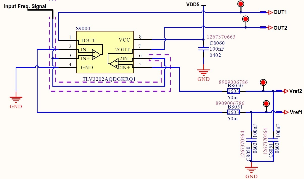
I have an issue in using TLV3202 as a comparator. While testing I supply Non inverting input (IN+) with frequency signal of 50% duty (Typically fat Low - 0V to High-3.3V levels) and Inverting input (IN-) with a reference voltage.

  • Circuit works as intended when Input voltage High level is more than the Reference voltage. I.e. Output same frequency with 0-5V level.
  • When reference voltage increased and made it more than input High level, the output supposed to be continuous 0V. But I get unintended pulse for ~100ns at each input pulse. This shall be observed from KHz to MHz range inputs and with almost 1.5V difference between input High and Reference voltage.

Circuit used for testing (Refer Only OUT1 comparator for below shown  cases and waveforms)

Case 1 : Input(Non inverting) = 0 to 3.3V, 100kHz, 50% duty, Vref1(Inverting Input) = 2.5V to 3.2V. (Tested for different reference and same behavior observed)

Result : Out1 as expected. Waveform below

Case 2 : Input(Non inverting) = 0 to 3.3V, 100kHz, 50% duty, Vref1(Inverting Input) = 3.5V to 5V. Tested at different levels and output is same as attached waveform. What could be the cause of this unintended pulse and how to overcome this?

  • Hi Selvakumar,

    it's very simple: The TLV3202 is a high speed comparator and you must treat it like a HF-OPAmp. So, you will probably need a solid ground plane, very shortest traces, suited filtering here and there and shielding. Please don't connect cables (or, even worse, wires) to the inputs unless you introduce 50R signalling. Provide a hysteresis and add an isolation resistor to the output of TLV3202 as shown in figure 30 of datasheet. And please don't directly touch anything of the circuit with the scope probe. Insert a 47...100R resistor first.

    You might want to use such a ground spring probe to avoid ringing:

    And, to avoid too much probe capacitance, take a 10:1 scope probe, no 1:1.

    Kai

  • Excellent advice, thanks Kai

    Chuck

  • Hi Kai,

    Thank you for your feedback. Layout points are taken care as you mentioned. I could add output isolation resistor but could you explain what is the impact of this?

    This unintended pulse is almost repeatable in all frequency inputs (<100 KHz to MHz) also, But in the measured waveform I see no distortion/noise. Can probing cause this repeatable error behavior?

    Thank you.

  • Hi Selvakumar,

    yes, improper probing can be the cause of these unintended pulses.

    Can you post the layout of your circuit? And can you show a photo of the setup?

    This so called "isolation" resistor has lots of effects:

    1. It decreases the short circuit current into stray capacitances connected to the node, when the voltage at this node is ultra rapidly toggling.

    C = Q / U = I / (dU / dt) 

    ->

    I = C x (dU / dt)

    So, an ultra fast change rate of voltage causes a huge current spike into the stray capacitance which can erode the signal ground, cause internal ground bounce and result in ringing and resonances across parasitic impedances (signal trace inductances, stray capacitances, etc.). Ground bounce can even make the comparator oscillate!

    2. It dampens ringing and resonances caused by undesired L C circuits formed by parasitic impedances.

    3. It isolates stray capacitances from sensitive nodes being inside of feedback loops and decreases the introduce of phase lag which would otherwise erode the phase margin.

    Kai

  • Thanks again Kai for your support of Selvakumar

    Selvakumar

    we actually characterize this family with very low overdrive levels (down to 20mV), so it very likely that noise coupling is causing the output glitches in your application.

    If they continue and you are unable to resolve with board modifications, Kai's suggestion of implementing external hysteresis may be required.

    Chuck

  • Dear Kai,

    Thank for your inputs. I will consider your recommendations and retest to check the behavior. I will share the layout after this measurement.

    since we are working from home, Measurement setup picture not readily available, I will share once we are back in office.

  • Good luck :-)

    Kai

  • We'll be looking forward to seeing the layout and measurement setup!

    Thanks again as always Kai for your help.

    Jonny

  • since this thread has no reply for last couple weeks, it will be closed.

    Please open a new thread once new information is available.

    thanks

    Chuck