This thread has been locked.

If you have a related question, please click the "Ask a related question" button in the top right corner. The newly created question will be automatically linked to this question.

THS4501: THS4501 as input level for RFSoC

Part Number: THS4501
Other Parts Discussed in Thread: THS4131, , THS4541, THS4551, BUF602, OPA690, OPA691, OPA820

Hey

My question is a little general but I'll give you more information if needed

I'm considering of using the THS4501 or the THS4131 as a input level for the ZCU29DR (Xilinx RFSoC), 
the configuration is single ended to differential converter with a topology of 2nd order high pass filter.

the VCM of the RFSoC (for AC coupling mode0 is 1.25V

my system frequancy is up to 25MHz

is it recomended to use it in that configuration?

BR

Elhanan

  • Why don't you use the much newer THS4541,

    Should work, what high pass cuttoff frequency? 

  • Hey

    thank you

    looks like THS4541 is better.

    pleas look at my input like this

    Vin = 1*sin(2*pi*f1*t)+0.1*sin(2*pi*f2*y)

    f1 = 10kHz

    f2 = 25MHz

    I need to separate the two signals before entering them to my ADC, so I'm splitting them and filtering them.

    1. one rail go to 100kHz HPF and then to the ADC1

    2. one rail go to 100kHz LPF and then to the ADC2

    I thought of using the op amps with 2nd order LPF and HPF configuration

    what do you think?

    BR

    Elhanan

  • So I think what you are saying is that these are both present meaning

    1. To get just the 10kHz you want a low pass to cut off the 25MHz

    2. To get just the 25MHz, you want a high pass to cut off the 10kHz? 

    I have done quite a lot more MFB LP filter work than HP work (although I do have that tool where I left it after I did it for the Intersil online designer

    So I could easily do the LP say at the 100kHz you mention, might want to use the THS4551 there as you don't need the speed of the THS4541, 

    1. Single ended input or differential

    2. Any gain

    3. Output to ADC - DC common mode, want to add a single pole there to make the overall filter 3rd order? 

    4. power supply desired

  • Hey Michael

    you got it right

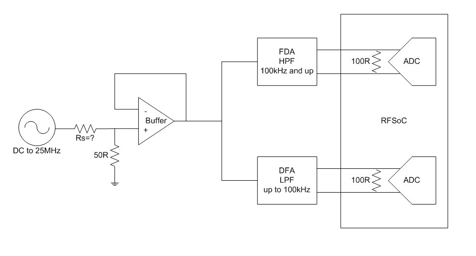
    if I would draw my system it will look like that

    1. My source is 50 ohm single ended input. I don't know my source internal resistance (it can change from source to source) so to avoid impedance control I think I need first stage, low noise, single ended op amp at buffer (follower) configuration, So that I can change the entry resistance simply by replacing one resistor
      1. it's input level  - 2Vptp, DC coupled
      2. BW of the input is DC to 100MHz.
      3. unity gain
      4. Power supply 0 to 5V.

    Can you recommend the OP AMP for that?

    1. After that the output from the first OP AMP split to two, one rail go to the HPF and one rail go to the LPF, assuming that the output impedance of the first OP amp is high, no need of impedance matching because of the split.
    2. HPF – the THS4541 you recommended looks good, can I use it as 2dn order LPF (I have managed to do so in TINA) or just as gain block with DC block capacitors in the input (like in the data sheet). also I want the ability to change the gain from 1 to 4 (by resistor change).
    3. LPF – to reduce my BOM complexity I refer to use the same OP amp like for the HPF, can I still use the THS4541 for that? Dose it support 2nd order LPF (did it in TINA). also I want the ability to change the gain from 1 to 4 (by resistor change).
    4. Dose the THS4541 suitable to 100 ohm load (my RFSoC), in the data sheet I saw only 500ohm designs.
    5. My system is very sensitive to noise.
    6. Regarding the output to ADC “Output to ADC - DC common mode, want to add a single pole there to make the overall filter 3rd order?” my prefer is to make the design hardware as simple as possible, no inductors if possible.
    7. No Power consumption sensitivity.

    BR

  • Here?are some comments/questions

    1. My source is 50 ohm single ended input. I don't know my source internal resistance (it can change from source to source) so to avoid impedance control I think I need first stage, low noise, single ended op amp at buffer (follower) configuration, So that I can change the entry resistance simply by replacing one resistor (you will have an uncertain attenuation here if you don't know the source R)
      1. it's input level  - 2Vptp, DC coupled (can't operate DC coupled with 0 to 5V supply on the amplifier, or is the source at some positive DC level)
      2. BW of the input is DC to 100MHz. (A 25MHz 2Vpp signal needs 157V/usec slew rate - 100MHz needs 628V/uscec, hard to find unity gain with that and low noise - look at BUF602, - unity gain stable VFA will have trouble doing that slew rate with low noise, OPA690 has slew rate, but poor noise - OPA691 CFA might be lower noise choice. )
      3. unity gain
      4. Power supply 0 to 5V.

    Can you recommend the OP AMP for that?

    1. After that the output from the first OP AMP split to two, one rail go to the HPF and one rail go to the LPF, assuming that the output impedance of the first OP amp is high (I think you mean low and yes driving right into an FDA based filter should be ok if we scale the R's to what it can drive), no need of impedance matching because of the split.
    2. HPF – the THS4541 you recommended looks good, can I use it as 2dn order LPF (I have managed to do so in TINA) or just as gain block with DC block capacitors in the input (like in the data sheet). also I want the ability to change the gain from 1 to 4 (by resistor change).(I think you mean the HPF here and yes you can do either blocking caps or active MFB, if you are changing gains and active ckt will require all RC's to change. This path needs to support the 25MHz 2Vpp signal?)
    3. LPF – to reduce my BOM complexity I refer to use the same OP amp like for the HPF, can I still use the THS4541 for that? Dose it support 2nd order LPF (did it in TINA). also I want the ability to change the gain from 1 to 4 (by resistor change). (this path is for the <100kHz signal, of course the THS4541 can do that but is overkill - again, if you go active filter all values change if you change gains)
    4. Dose the THS4541 suitable to 100 ohm load (my RFSoC), in the data sheet I saw only 500ohm designs. (your ADC is internally terminated by a differential 100ohm load? What DC common mode V does it need. Also, pretty much all ADC's like to see a final diff cap which then requires an isolating R from the FDA outputs - no L's. What Bandwidth would like to set that RC to where there will be a bit of insertion loss to the 100ohm diff R say using about 10ohms on each output side.)
    5. My system is very sensitive to noise.
    6. Regarding the output to ADC “Output to ADC - DC common mode, want to add a single pole there to make the overall filter 3rd order?” my prefer is to make the design hardware as simple as possible, no inductors if possible.
    7. No Power consumption sensitivity.

    BR

  • Oh I see way at the top the CM voltage for the ADC is 1.25V. that will be fine for the THS4541 operating even on 3.3V supply. That would be set of course with the CM control input and would stay the same as you changed gains. 

  • Hey Michael

    Thanks so much for the quick and detailed answers

    I can see that you don't recommend to use single ended buffer in the entrance, because of noise/performance

    if so, the meaning is that I will have to consider the parallel input impedance of the two FDAs that I have and by that to set the Rt termination resistor

    should I do it by using formula (11) from the data sheet of the ZA of the HPF parallel to the ZA of the LPF ?

    are the blocking caps transparent (dose they become short circuit) for formula 11 ?

    dose the low frequency signal will only see the input impedance of the LPF? (because of the blocking caps of the HPF)?

    Yes my ADC is internally terminated by 100 ohm. Can I sent you my tina simulation of the system (after I will have it..), So that you can express your opinion?

    BR


  • Well yes, you will have the active input impedance of each channel to consider, being an active filter that will also change with frequency. Anything wrong with the BUF602 idea on +/-5V - your signal is 2Vpp max, on what DC level? 

    I am trying to answer all that will need to be answered before I spend too much time in my LP MFB design tool. 

  • So here I took a run at a 100kHz active filter, inserted a slight loss in the output to add a cap. All ADC's would like to see a differential and often single ended caps at the inputs - the sampling edge is very fast and you need those caps to absorb that edge without getting into the amplifier output impedance. 

    I did this as a 3rd order Butterworth, which made that last cap pretty large, can just go 2nd order in the filter and push that final RC pole way out with a much smaller cap 

    Here are the responses

    Here are the noise at output and then after RC filter - all active filter have noise peaking, that RC helps a bit, 

    And then the file, 

    100kHz active filter with THS4541.TSC

  • Hey Michael

    first of all - Thank you for your effort.

    I have some questions regarding to it

    1. how did you calculated the input impedance of this network (ZA) with formula 11?

    2. can you again explain the 10 ohm resistors in the output?

    3. can you do 2'nd order HPF (or BPF) with more than unity gain?  (lets say gain =2 V/V, i tried in the web designer but it always adds another amp for gain level)

    BR

    Elhanan

  • Well Elhanan, you have marked this resolved? Or someone did, 

    Did you want to open a new one with the THS4541

    Well the input impedance is going to change, but at low frequencies I think it is following that equation I did many years ago now, here is the input impedance simulation. this is 2.4kohm at low F then 609 ohm at higher F. I was still thinking you needed something like the BUF602 to drive this. 

    The 10ohm inside the loop is something we found later to help isolate the reactive open loop output impedance of these RR output device when you have to drive a feedback cap. The 10ohm outside the loop are needed to isolate the cap load for stability.

    The HP design is something I have not looked at for years, would need to find those design files - that one is intended to pass the 25MHz signal, why not place the HP at say about 18MHz. will give you more rejection for the lower F signal. 

  • I was able to get a HP filter out of filterpro and adapted it an FDA, I am getting about a 16MHz corner with a 5.2dB gain at 25MHz, I did not adjust that last RC yet. 

  • Hey Michael

    1. I accidentally marked the thread as resolved.. still need you..
    2. to solve the input impedance problem I will use a buffer like your recommendation.
    3. I have one concern about using MFD network internal gain/attenuation, because change in the gain/attenuation requires changing all the components in the MFB, however if I'm using second amplification stage (that make it easier to make modification on the board) I can see that my total output noise larger in 10^1 order (pleas see my Comparison have attached of one stage MFB vs two stage MFB (separate filter and gain level) for Gain = 10 and 1MHz cut off), maybe there is a better way to do it?
    I will still need you to examine my final design if that is OK with you.
    BR
    1122.Cascade.TSCsingle_with_gain.TSC

  • Well it looks like you are getting an MFB high pass out of webench, I had trouble with mine in that those nodes with all caps coming in caused a sim failure which is why I put 100k to ground on them. 

    Yes, if you need to vary the gain a non filter stage would be easier - why don't you do that before the FDA filter stage with a single ended op amp - maybe the OPA820? 

  • actually, if you need a gain of 10 and 25MHz, the OPA820 is not fast enough. need maybe at least 400MHz GBP - if you wan that to be the same part for gain of 1 and 10, unity gain stable isneeded

  • Hey Michael

    regarding the Error - I had it to, I found the solution in the forum, it related to caps in series.

    go to Analysis Parameters, press the pointing hand icon => view all, in the shunt conductance you put 1p (if i'm remember right).

    regarding to gain:

    1. I can't amplify before the MFB HPF because I have another signal there that going to the MFB LPF that I need to attenuate. also my low freq signal is 1V and I don't want to amplified it to 10V.

    2. what is unity gain stable?

    3. the question is what is better regarding noise performance vs modification simplicity

    3.1 FDA in an MFB HPF configuration that include gain.

    3.2 FDA in an MFB HPF configuration with unity gain + another (simple single feedback) inverter FDA for gain level.

    thank you 

  • Looking just at the output noise for the MFB at the twogains, they seem to be about the same?? I have not worked on HP MFB for maybe 8years, this is unusual but that is what the sims show.So yes, if you take the same output noise for the gain of 1 filter and gain it up by 10X, that is going to be a lot of noise vs putting the gain in the active filter - I am mystified, 

  • Here is the gain of 10 1MHz filterpro design adapted to the THS4541, I had the min conductance parameter set to 1p, didn't help still needed the 100kohm which physically I kind of like as who wants floating caps on the board. 

  • Hey Michael

    thank you very much for your effort

    pleas look at my "final design" that utilized

    1. input buffer

    2. 2nd order Bessel HPF 1MHz 20dB gain MFB 

    2. 2nd order Bessel LPF 100kHz -10dB gain MFB 

    will be happy to get your feedback

    thank you

    BR

    HPF_LPF_BUF.TSC

  • Morning 

    I looked again at the HPF flatness, took the 100ohms back out (0ohm) and it was fine, here is that HPF response with 0ohm (flatter) and 20ohm, perhaps that is a better value to help stability of the BUF602 

  • Thank you Michael

    I have note it all

    Last question that I have 

    My ADC (RFSoC) stage absolute maximum rating of input voltage is 2.1Vptp (Vcm=1.25) with 100ohm internal termination.

    so in order to provide protection from the THS4541 I thought of using it with 0-2.7V instead of 0-5V V Supply and then the 20ohm that you add in the output can protect the input voltage to the ADC from exciding 2V (by 100/140 voltage divider)

    can you recommend that?

    thank you

  • so your absolute swing is 0.725 to 1.775 on each side 180deg out of phase, 2.7V might work but that is getting to edge of operation, what is you ADC supply

  • Hey Michael
    according to my device (RFSoC) data sheet ds926

    Vadc_avcc = 0.925V

    Vadc_avccaux = 1.8V (that should be the input buffer)

    Tank you