This thread has been locked.

If you have a related question, please click the "Ask a related question" button in the top right corner. The newly created question will be automatically linked to this question.

PGA309: PGA309: PGA309 Communication Failure at High temperature

Part Number: PGA309

Hello

Based on the inputs  on the previous thread , we are considering changing the TVS diode on PRG pin to SMF5.0A.

I have a query  on the datasheet parameter of PGA309. absolute maximum ratings of the PGA309 mentions

Supply Voltage, VSD, VSD +7.0 V

Input Voltage, VIN1, VIN2 , (2) –0.3 to VSA +0.3 V , in our design VSA is5V, still maximum allowed voltage on the Vin & Vin 2 is 7.30V ? or will it be like 5V+0.3V ? Is this applicable on PRG pin also ?


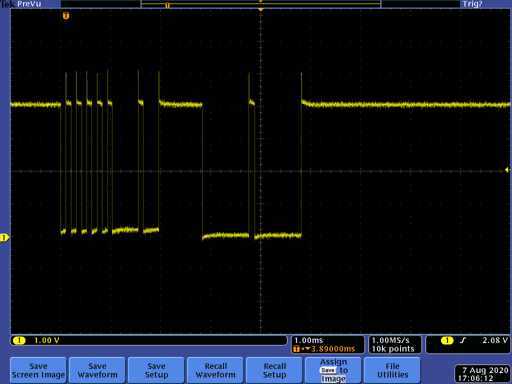
for now, we have seen another failure which is of same nature. and it works perfectly below 115C.
In addition is there any possibility of the analyzing the Failed samples at die level by TI . do you have any process to take these samples and do a quick analysis on them?

Let me know your thoughts please.


thanks,

Raghavendra


  • Hi Raghavedra,

    The maximum operating voltage supported by PGA309 is 5.5V maximum from -40C to +125C as shown on the electrical characteristic table on page 7. The device is not intended to be used with a supply voltage of +7V; the Vs=+7V Absolute Max Rating of the supply voltage only represents the maximum voltage the device can tolerate during a fault without permanent damage.

    In general, the inputs of the device should not exceed the supply by 0.3V or -0.3V below GND, if the voltage is exceeded then the current should be limited to less than 10mA during the fault. 

    Page 92 of the PGA309 user guide, discusses the electrostatic discharge (ESD) internal cells of the PRG pin and over-voltage protection in great detail.  The internal ESD diodes can handle up to 10mA continuous load. However, the internal SCR1 structure can trigger during an over-voltage fault, keeping 80mA of sustaining current, as Figure 4-18 shows. If the current is not limited, the voltage will increase again; this increase, combined with higher currents, may cause permanent damage to the ESD cells and make the PRG circuitry unusable. 

    Figure 4-20 and Figure 4-21 on the PGA309 user guide, have the recommended protection circuits which include series resistances, protection diodes and parallel capacitance and EMI filtering for robust protection.

    Please provide a PRG digital communication when the issue occurs to verify both the timing in the communication and for intermittent connections.  Keep in mind, if the timing is slightly outside spec or marginal, the communication issue can manifest itself at hot temperature.  If there is no intermittent connection issue or marginal timing issue on the 1-wire interface at hot temperature, then it may be possible that the internal ESD structure may have been damaged or degraded by an over-voltage or ESD event, manifesting the issue at hot temperature.

    Did you purchase the PGA309 device via a distributor?

    Thank you and Regards,

    Luis 

  • Hello Luis,

    It took a while capture the Waveforms as the Device with failure was at Factory. so we have captured the waveforms at 25C and 125C and attached the both waveforms for your review.

    Please kindly go through the attached file and let me know your feedback. All I can see is that there is some dip in the Response byte received from PGA.

    On other had, we are in discussion with the our PCBA vendor to get us the Purchase details of this part.Waveforms.docx

  • Hi Raghavendra,

    Thank you for the PRG waveforms.

    The PGA309 output low level for the PRG pin is expected to be less than 0.4V with respect to the PGA309 local GND pin. 

    The PRG pin is an open drain, and the output low level specification is 0.4V while sinking 5 mA.

    I have a couple of questions:

    1) The waveform document mentions the oscilloscope capture is placed near the PGA309 PRG pin.  Is the oscilloscope probe referred to the GND pin of the PGA309 or the controller GND?  Is there any voltage potential difference between the GND of the controller and the GND of the PGA309?

    3) What is the value of the pull-up resistor on the PRG pin?

    4) In other units that do not show the communication issue, do they also show this low-level voltage higher than expected, 0.8V at 25C and 1V at 125C?  or is the behavior only present on the failing device? 

    5)  I have a small portion of the schematic from the previous post.  Is it possible to share a complete schematic?  I assume this is a 4-wire connection, please show a diagram of the digital interface connections, including VCC, PRG, VOUT and GND, and how this interface/connect to the controller.

    For your reference, information on the return process and the failure analysis process is below.  However, it is probably best to verify the above prior proceeding.

    Customer Returns

    Failure Analysis

    Thank you and Regards,

    Luis

  • HI Raghavendra,

    I have not heard back from you.  If you have further questions, please feel free to reply or start a new Forum request.

    Thank you and Regards,

    Luis

  • Hello Luis,

    Please find my response below for your questions.

    1. Yes, oscilloscope waveform refereed between the PGA309 & PGA309 Gnd.

    3. We dont have any pull-up on our board, But we are utilizing the internal pull-up on the TTL-232R-5V-WE. (The PRG pin is used only once  in production while calibration of the device.)

    4. I captured the waveform of one working device as it & added a 3.9kOhm pullup on our board and did not notice any major change in the signal(low level). The waveform is attached in the Document

    5. Schematic is attached for your reference. No we are using 1 wire communication.

    Let me know your thoughts on this.If you need any further data, or testing from my side please let me know.Schematic_PGA309_Raghavendra.docx

    (Because of Covid19 situation I am not able to access the lab easily hence there will be some delay in my response.)

    thanks,

    Raghavendra 

  • Hello Raghavendra,

    The only unexpected behavior is that the response does not reach zero level and is around ~0.8V for a zero bit at the PRG pin output.  It is strange that the behavior is systematically occurring on all devices.  One thing that comes to mind is a grounding issue, or GND voltage differential from the controller GND to the PGA309 GND connection.  When you captured the oscilloscope plots above, did you place the oscilloscope probe right at the PRG pin 12 and right at pin 11 (GND D) of the PGA309 device, with the oscilloscope probes making direct contact with the pins of the PGA309 device?

    Below is a plot of the observed PRG pin behavior on the PGA309EVM.  I placed the oscilloscope probe on the PGA309 side, connected directly to pin11 and pin 12 of the PGA309.  When looking at the difference between the zero level from the controller and PGA309 PRG output low level response, the PRG VOL level is close to zero volts and the difference in low level between the controller and PGA309 is less than 200mV. Per the datasheet, the maximum output low level VOL for the PRG pin is 0.4V; and the PGA309EVM produces a low level below this voltage on the PGA309EVM.  Please see below.

    Thank you and Regards,

    Luis


  • Hello Luis,

    Even I tried communicate with the same units through the TI PGA309EVM and the waveform was as expected.


    I am yet to conduct same testing on those devices failed to communicate  at 125C. But seems like the issue is related to the 5V TTL USB convertor.

    thanks a lot for your support.

    regards,

    Raghavendra