This thread has been locked.

If you have a related question, please click the "Ask a related question" button in the top right corner. The newly created question will be automatically linked to this question.

TLV9152: op amp cuts off when PWM duty cycle < 4%

Part Number: TLV9152
Other Parts Discussed in Thread: LM7705

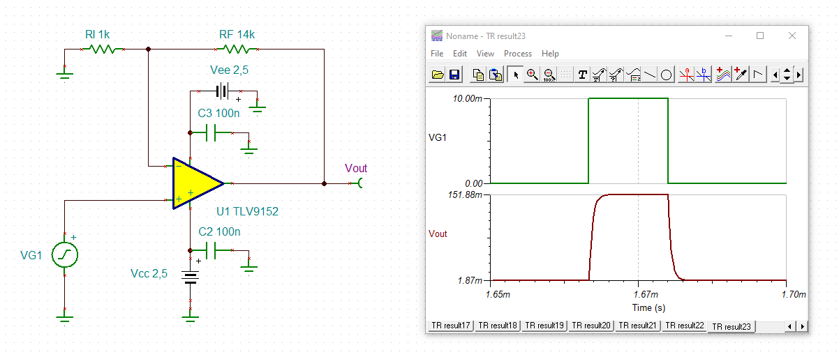
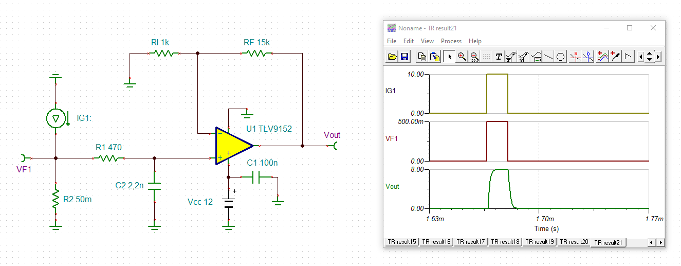
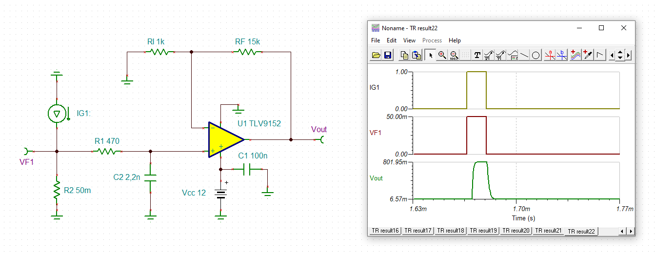
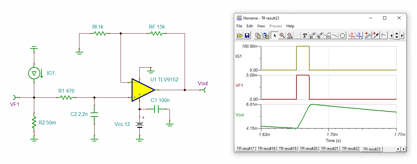
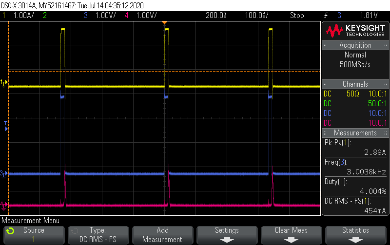
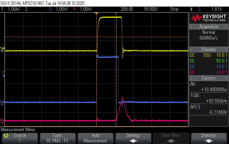
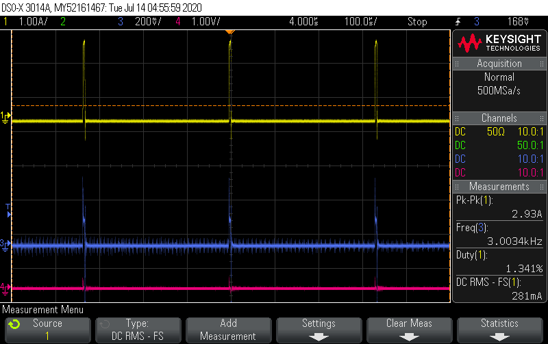
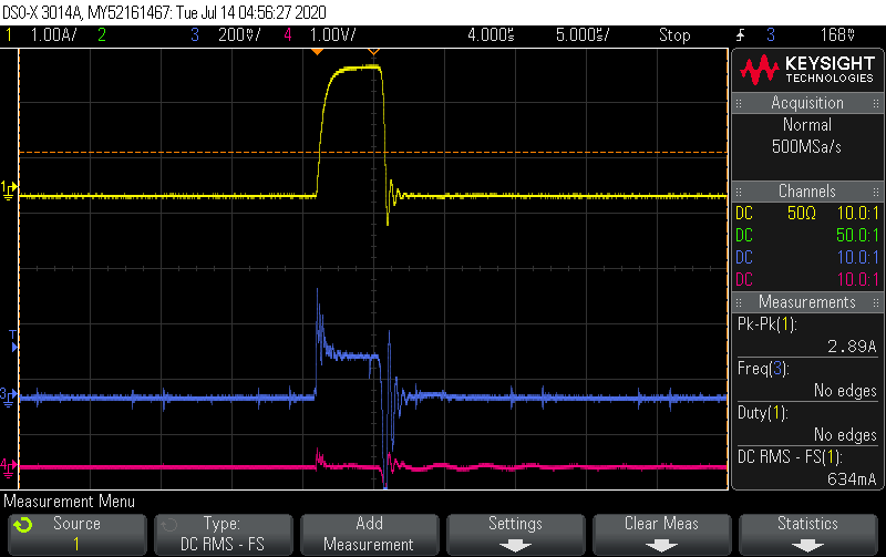
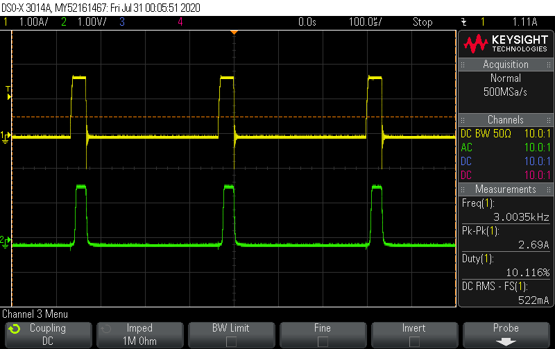
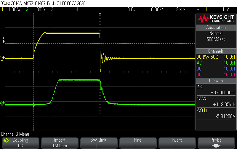
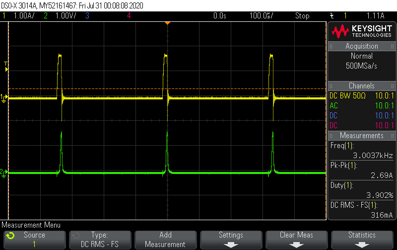
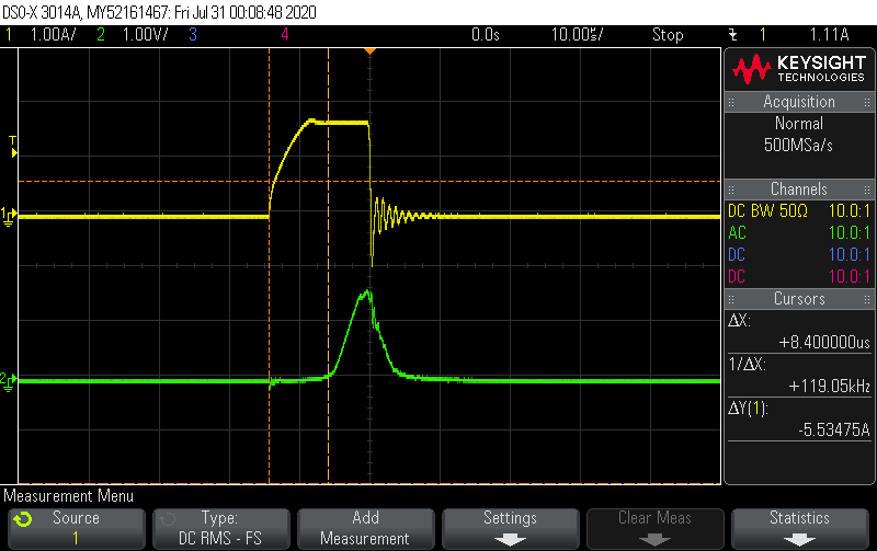
I am using this part as 15 gain amplifier for sensing the current through a load.

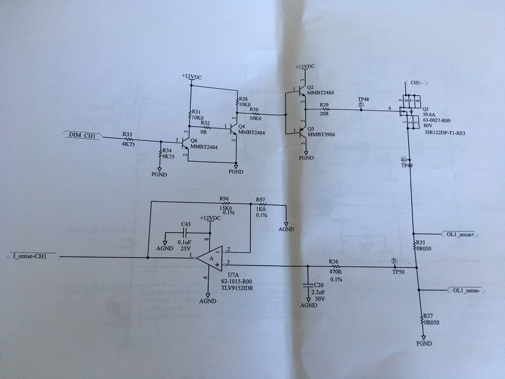
Based on an analog 0-10V input, the microcontroller outputs a PWM duty cycle to the LED load; the current is permanently monitored and the value is read through a sense resistor, and amplified to the micro as I-SENSE_CH1 (on sch attached)

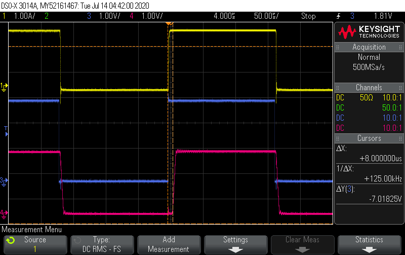
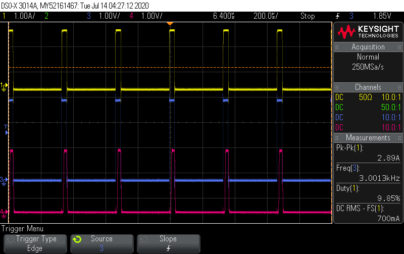
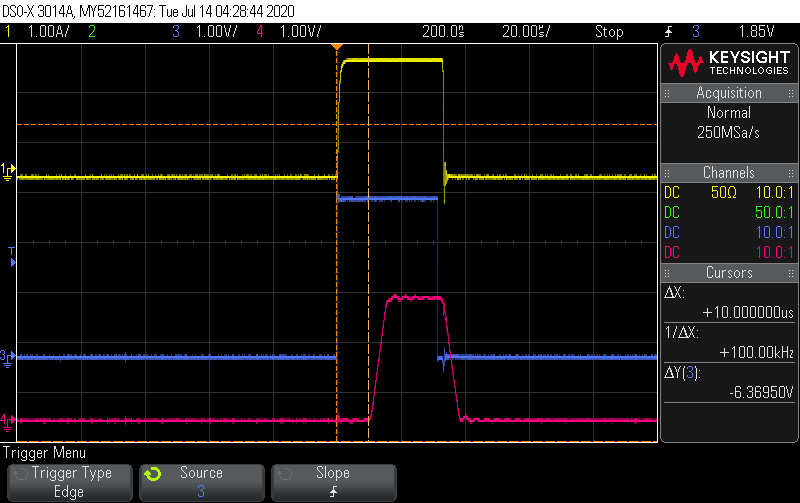
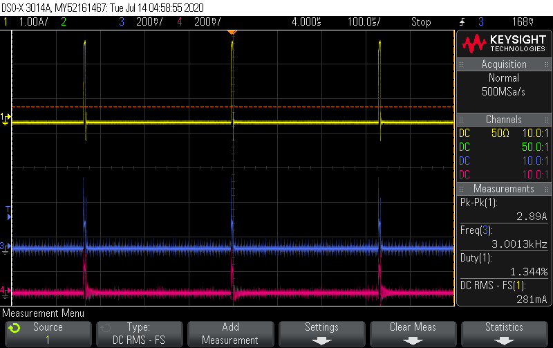
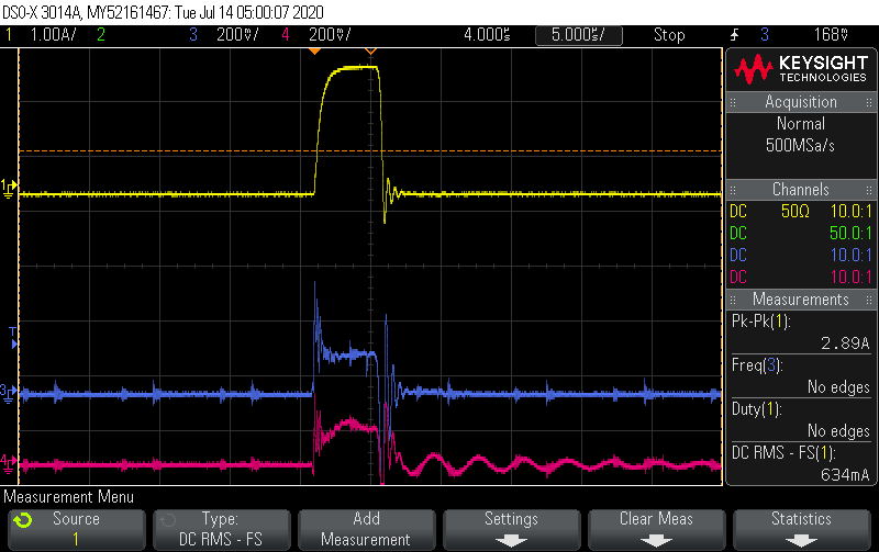
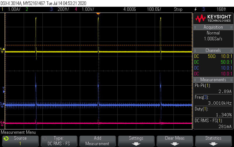
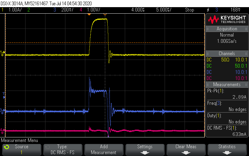
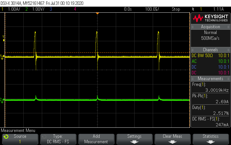
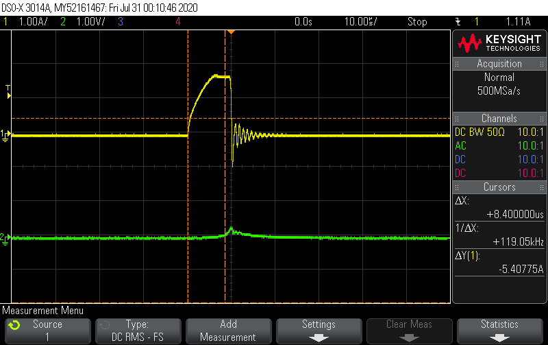
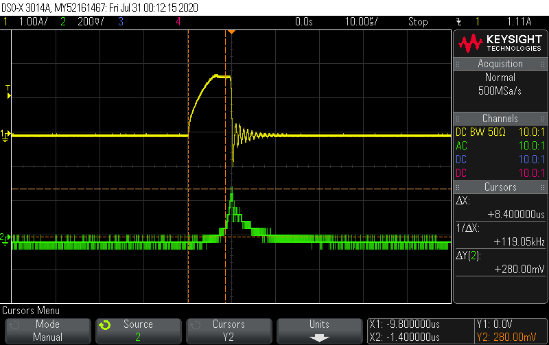
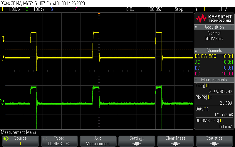
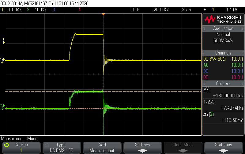
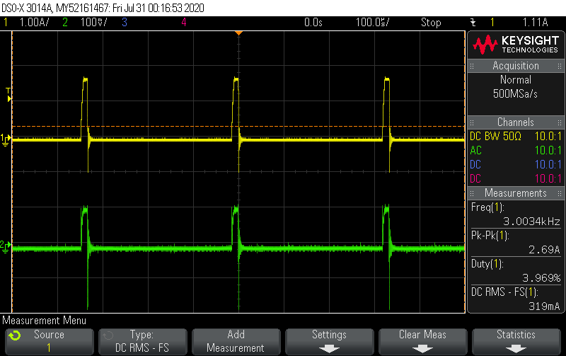
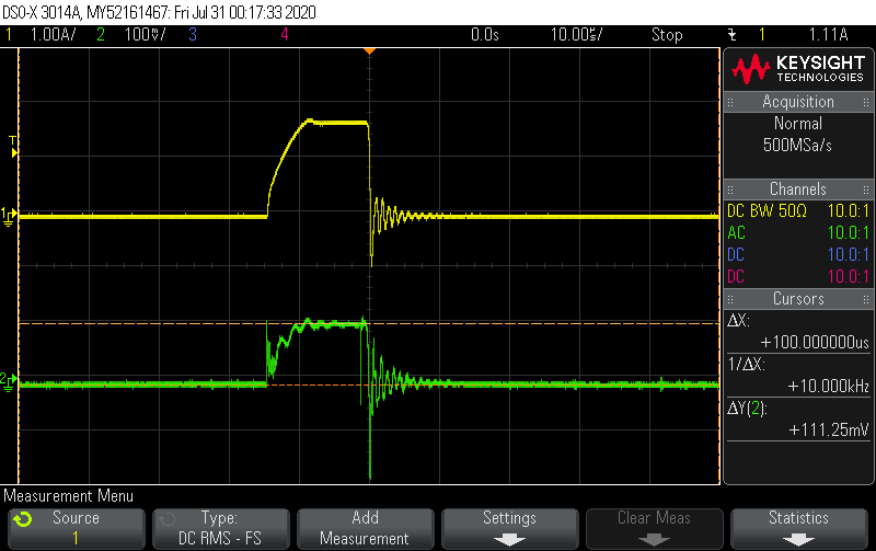
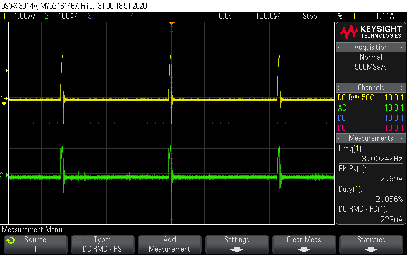
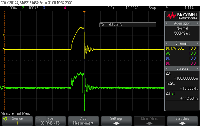
Everything works well, except for when PWM<~4% the output of the op amp cuts off; also it looks as it is delayed

Here is the schematic: 

Also 

I can send some scope shots through email,  taken at 50% duty cycle, 10% and 4%

I could not attach here. For some reason does not work.

Thank you


  • Hi Mariana,

    Can you please try attaching the schematic and scope shots again? To attached an image please use the icon "Insert/Edit Media". Please see below.

    What is the frequency of the PWM signal?

    Depending on the PWM frequency the issue may be that amplifier does not have enough time to respond to the change in input signal. For example, for a 1kHz 50% duty cycle PWM signal the amplifier has about 500us to respond but at 4% duty cycle the output only has 40us to respond.

    The delay you mentioned might be due to overload recovery, but I will know more once I see a schematic and scope shots.

    Thank you,

    Tim Claycomb

  • Hi Tim, thank you for your reply.

    Unfortunately I have a family emergency in Toronto, and I had to take off this week.

    I don’t have the laptop with me.

    The frequency is 3KHz

    Could you tell me at this freq what response is possible?

    If this part is not good, which part would do the job?

    Thank you

  • Hi Mariana,

    the TLV9152 would be fast enough for 4% duty cycle:

    mariana_tlv9152.TSC

    So I think you might have an issue with input or output saturation because your input or output signal is too close to the supply rails. Because of this seeing the schematic and the scope plots would be essential for being able to help.

    Good wishes for your family issue :-)

    Kai

  • Hi Mariana,

    What are the supply voltages of the op amp? Does it use a single or dual supply?

    What is the amplitude of the PWM signal? For example, 0-5V, 0-3.3V, etc.

    If single supplies are used, the issue is likely due to overload recovery and slew rate.

    If you can remember what the schematic looks like you could try drawing it on a piece of paper and taking a picture. 

    Please spend time with your family, we will be here when you return.

    Thank you,

    Tim Claycomb

  • Hi Tim,

    I finally found a picture of the sch, and here it is,

    Dim ch1 is the PWM signal from the micro at 3.3V.

    Opamp is single power supply 12V.

    I hope you can have now a better idea.

    Thank you,

    Mariana

  • Hello Mariana,

    I have created a TINA simulation file for the schematic you provided. The transistor models used in TINA may be different from what the schematic specified, so the exact output results may differ. Let me know if there are any discrepancies between your paper schematic and that which is in TINA.

    Simulation File:

    TLV9152_E2E.TSC

    In running the simulation file, I do not see any issues with a 3kHz pulse train with a duty cycle of 4%. If you are able to send scope shots of the output behavior I would be able to better understand what issues may be present. 

    Note, in the first post you mentioned the circuit is designed to have a gain of 15V/V however in its current non-inverting configuration, it is at 16V/V. the difference may introduce output swing issues as the desired output may be beyond the supply rails of the amplifier. 

    I hope you and your family are doing well,

    Regards,

    Jacob

  • Hi Mariana,

    what is your LED current?

    mariana_tlv9152_1.TSC

    Kai

  • Hi Kai,

    The channel holds max 100W at 48V, so the max current is just above 2A.

    Thank you so much,

    Mariana

  • Hi Mariana,

    With 2A flowing through the sense resistor we should see able to see something close (or better) to the simulation that Kai showed with an 800mA current. I think the best way to help determine what is happening is to see scope shots of some measurements. Hopefully this can wait until you return to work. If not, maybe a co-worker can send post them.

    Thank you,

    Tim Claycomb

  • I will return Sunday evening to Vancouver.

    I will send scope shots images when I get home.

    Thank you so much, your help is really appreciate it.

    Mariana

  • Hi Mariana,

    I look forward to the scope shots. Have a safe trip!

    -Tim Claycomb

  • I am back in Vancouver.

    I attach the scope shots I have.

    I hope this will help to resolve this issue.

    At duty cycle = 50% here is the scope shot; CH1 (yellow) = load measurement by probe current;  CH3 (Blue) is the PWM from micro, CH4 (violet) is the I_SENSE_CH1 (output of opamp)

    At 10%:

    At 10% zoomed in, and delay:

    At 4% duty cycle:

    Zoomed in at 4% and delay:

  • Hi Mariana,

    Thank you for the scope shots!

    Would it be possible to see measurements of the output voltage, PWM signal, and the input voltage of the op amp (measured at TP50 on your schematic) measured at the same time?

    Thank you,

    Tim Claycomb

  • Tim,

    I am working from home due to COVIDt, and because I travelled to Toronto I can not go to the office now, maybe night time when nobody is there.

    But, I have in my computer few shots taken on these points.

    Here they are.

    I took them at 1% duty cycle. CH1 is load, CH3 is TP50, CH4 is output of opamp

    Zoomed:

    Also, I have some shots taken at dc= 1% when I changed R36 fro 470R to 270R: CH3 is at TP50, CH4 is at Pin3 (positive input in opamp)

    And zoomed in:

    Also I have some images taken for the existing R36 =470R, at dc=1% where CH3 is TP49 and CH4 is output opamp:

    And zoomed in:

  • Hi Mariana,

    I think some of the issues you are seeing may be related to the RC filter at the input of the op amp (R36 and C26). One time constant of the RC filter is 1.034us, it will take about 3.1us just for the cap of the RC filter to charge to 95% of the input signal. When you get back to the office would it be possible to remove C26 to see if the delay goes away?

    Thanks,

    Tim Claycomb

  •  Hi Tim,

    Today I am in the office.

    Took out C26.

    Here you have the scope shots, and you'll see that the delay remains now at~8.4us. But the shape of the output from the opamp is no square shape, and I remember now that was the reason I added the cap.

    I have the images for the output of the op amp for dc=10%, 4% and 2.5% (at this value is already cut off).

    I also have the images for the input in the op amp (pin 3) at 10%, 4%, 2%.

    Output op amp (CH1 = load, CH2= outopamp)

    dc = 10%, and zoomed

    For dc= 4%:

    For dc= 2.5%

    For input in the opamp:CH1 = load, CH2 input at pin3

    For dc = 10%

    For dc = 4%

    At dc = 2%

    So, I hope you can find a solution for our problem. We are close to order the new spin of these boards, and need a solution.

    Thank you,

    Mariana

  • Hi Mariana,

    one problem arises from the fact that you have different grounds AGND and PGND. You should improve the ground management so that there's less parasitic inductance and by this less ringing between these grounds.

    C26 is too big, as Tim already mentioned. I guess that you can take a much smaller C26, if the ground problem is eliminated.

    And, last but not least, there is an overload recovery time issue in your circuit. The output of U7A saturates after it swings to the negative rail and can leave this area only with a delay. So I would add a small negative supply voltage to U7A, for instance by the help of LM7705.

    Kai

  • Hi Mariana,

    I agree with Kai regarding the GNDs. Another thought is that there might be a voltage potential difference at the GND connection of R97 which is causing an increase in negative offset voltage to your circuit. This could increase the overload recovery because the output is slammed to the negative rail for a longer period of time. 

    The input to the op amp (without C26) appears to go well below GND which is not good. This can damage the op amp if the absolute maximum ratings are violated.

    Is it possible to add a -4V supply to the device (for testing purposes only) to see if the issues go away? This can be done by cutting traces or lifting the pin of the device and connecting a wire to it.

    Thank you,

    Tim Claycomb