This thread has been locked.

If you have a related question, please click the "Ask a related question" button in the top right corner. The newly created question will be automatically linked to this question.

OPA445: OPA445 schematics

Part Number: OPA445
Other Parts Discussed in Thread: LM3886, , TINA-TI

Hi,

Why this type of assembly is stable.

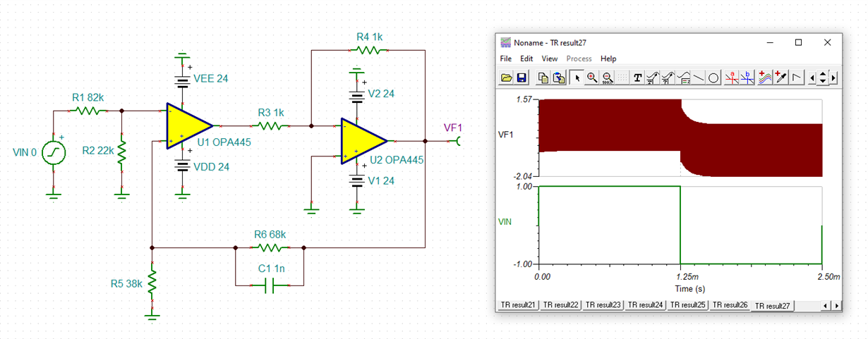
The counter-reaction is done on the + pin of U3 knowing that U4 has a gain = -1

Normally any feedback on the + pin of an AOP does not allow it to operate in a linear mode.

The equations of such an assembly give :Vout1=- Vin1*(1+R36/R32)

Do you have an application note that explains this mode of operation?

Thank you for your help

  • Hi Druilhe,

    where did you find this circuit?

    druilhe_opa445.TSC

    Kai

  • it's a setup used on amp cards.

    The simulation shows that it works...!

    We find the same schema on the lm3886 datasheet

  • See figure 2 of the attached documentSchémas 1.pdf

  • Hello Druilhe,

    An op amp's open-loop gain/phase and output impedance vs. frequency characteristics in conjunction with the actual circuit implementation must be fully considered and designing an amplifier circuit for assured stability. The OPA445 is a precision HV op amp with about a 15 mA output current capability,  while the LM3886 you mention is a High-Performance 68W Audio Power Amplifier. They are completely different amplifiers, having completely different dc and ac characteristics and uses. If the two-amplifier circuit that you reference was deigned and correctly compensated for use with the LM3886, there is absolutely no assurance that the circuit will be stable with an OPA445, or any other op amp. The circuit must be designed so that the ac characteristics's of the particular op amps being used are fully considered.

    Kai did a nice job demonstrating using TINA Spice that the two-amplifier configuration you propose is unstable. Likely, the circuit could be redesigned to be stable using the OPA445 op amps; however, the full circuit operating and conditions would need to be known before that work should commence. Additionally, I am not really sure that the circuit function couldn't be satisfied with just one HV op amp. It looks like the application just needs a non-inverting gain of about +2.8 V/V which could be satisfied with just one OPA445 op amp.

    Regards, Thomas

    Precision Amplifiers Applications Engineering

  • Hello Thomas,

    I agree with your analysis however if you look at figure 2 of the attached document (Schémas1.pdf)  the counter reaction is on the + pin of the AOP. Which is shocking.

    The idea of putting 2 AOPs in series is to simulate the same operation as schematic 2. This may not be a good idea.

    However, this counter-reaction on the + pin of the AOP in diagram 2 is suspicious.

    Do you have an idea?

    Regards Yvan.

  • Hi Yvan,

    you said that you did find the same scheme in the datasheet of LM3886? So you mean the "DC Electrical Test Circuit" from page 5?

    Well, this is a simplified schematic of the standard test circuit which is used since decades in the OPAmp industry to test input offset voltage, input bias current, input offset current, open-loop gain, common-mode rejection, gain-bandwidth product, etc. All use the same test loop with only slight variations. What you have overlooked is the "NULL" in the second OPAmp. It means that this OPAmp forms an integrator :-)

    So a less simplified schematic of this standard test loop looks like this:

    Kai 

  • I'm okay with what you said.

    See attached schematic my question remains the same why the assembly is stable with a feeback on the + pin of the AOP.
    The simulation shows this stabilityMontage AB.pdf

  • Hi Yvan,

    Certainly the feedback in an op amp circuit needs to be predominantly negative to assure stability. Most single op amp circuits use only negative feedback and load conditions that assure a stable operating case. The Improved Howland Current Pump (V-to-I converter) is an example of a single op amp circuit that uses both negative and positive feedback, but the predominant influence on the circuit that keeps it stable is the negative feedback.

    Once additional components are added to the output of an op amp circuit either within, or external to the feedback loop additional phase shift is added to the loop which can degrade the phase margin and destabilize the circuit. Adding a second op amp within the loop as in the LM3886 circuit you reference adds much phase shift into the loop. Very likely the feed back to the usual inverting input in that case would reduce the phase margin to the point where the circuit is unstable. That is where the reversal of the two op amp inputs comes about in the LM3886 test circuit. The second amplifier adds so much phase shift to the loop that the function of the inverting and non-inverting inputs is switched. Doing so, the phase margin can be reestablished to good positive value such as ~45 degrees and the circuit is stabilized.

    Often, and I suspect this the case for the LM3886 there are additional poles and zeros in the two-amplifier loop that degrade the phase margin. A very careful Bode analysis of the circuit must be accomplished to see where they occur and what needs to done to the circuit to make sure the circuit is stable. Looking at the LM3886 Figure 1 circuit, I expect that the 220 pF capacitor across the first DUTs inputs, the parallel 0.7 uH and 10 Ohm combination at its output and the capacitor that Kai proposes adding across the null amplifier input and output, are the necessary additions to achieve stability. Note that these are in addition to the reversal of the DUT amplifier's inputs seen in the circuit schematic.

    As I mentioned previously, the OPA445 and LM3886 are completely different amplifiers with completely different electrical characteristics and intended uses. Do not expect that the same compensation techniques will necessarily work for the circuit comprised of OPA445 op amps. The compensation may need to be very different.

    Regards, Thomas

    Precision Amplifiers Applications Engineering

  • Bon jour Ivan,

    can you draw your schematic in TINA-TI? Then we could do some simulations for you.

    Kai

  • Hello Kai,

    You will find the design under tina.
    On the other hand I do not know integrated new model of transistor the 2N5667 and the 2N5416.

    I replaced 2N5667 with 2N5769 and 2N5416 with 2N5447.

    Thank you for your help

    Ampli_OPA445.TSC

  • Hello
    You will find enclosed the TINA design of the amplifier.

    5672.Ampli_OPA445.TSC

  • Hello Yvan,

    Thank you for the TINA file for the OPA445, plus output stage circuit. You note on the schematic that the "Input 24 V Output 16 V positive feedback OPA445." Actually, as I explained earlier the feedback to the OPA445 non-inverting input results in negative feedback due to all the phase shift through the output stage and RC networks in the feedback loop. You can see that the feedback is indeed negative if you run a simulation and note the relationship of the phase at the OPA445 inputs and its output.

    The circuit points in the diagram below illustrate the phase at each of them:

    • VIN - Signal generator input to the circuit
    • Vinv - Signal level at OPA445 inverting input
    • Vo1 - Signal at OPA445 output
    • Vo2 - Signal at output of entire amplifier circuit
    • Vnin - Signal at OPA445 non-inverting input

    It is evident from the diagram that the signal at the OPA445 non-inverting input (Vnin) is close to 180 degrees out of phase with the OPA445 output (Vo1). Therefore, even though the feedback loop connects to the non-inverting input, the feedback is inverted from the input signal. Thus, the feedback is not positive and the circuit remains stable because of negative feedback.

    Regards, Thomas

    Precision Amplifiers Applications Engineering