This thread has been locked.

If you have a related question, please click the "Ask a related question" button in the top right corner. The newly created question will be automatically linked to this question.

LMH6552: About differential output voltage error of LMH6552

Part Number: LMH6552
Other Parts Discussed in Thread: THS4541, LMH6554

Hello,


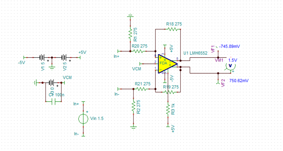
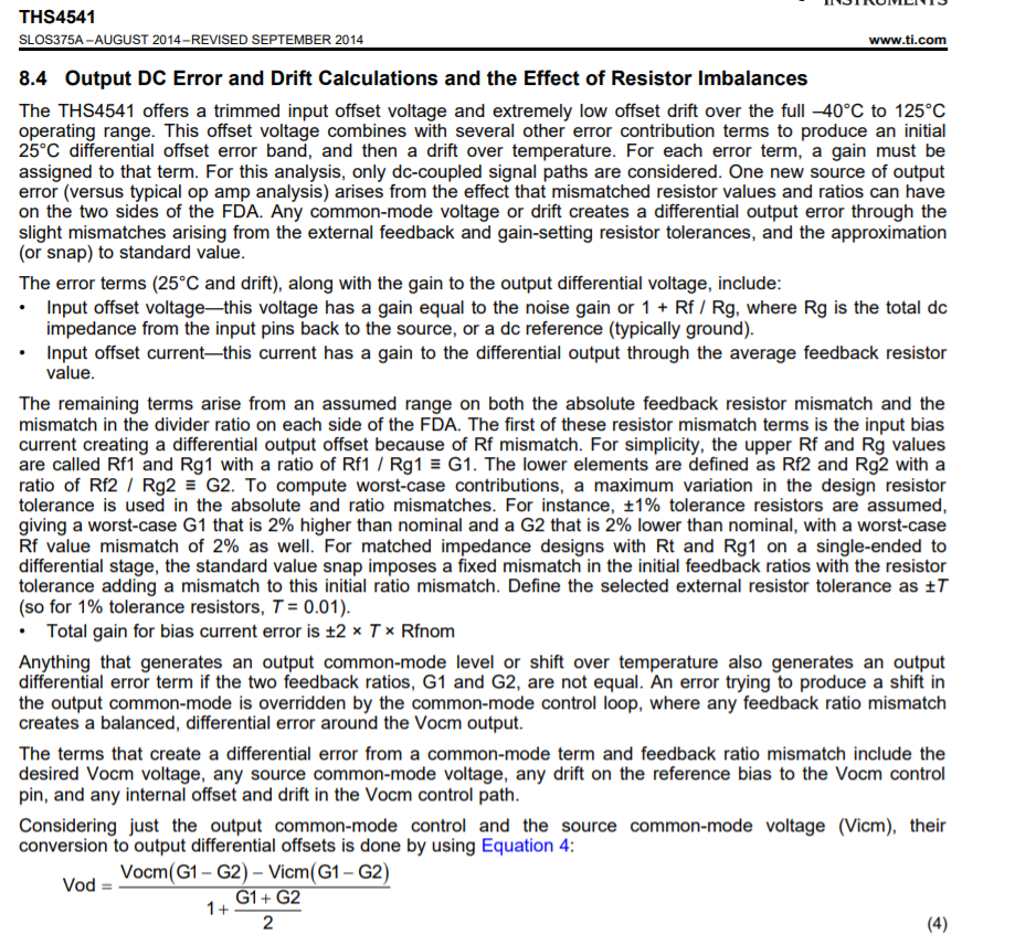
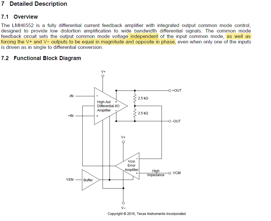
Customer use a full differential operation amplifier LMH6552. In practice, there is a error between out+ and out-. I use TINA to simulate the FDA LMH6552, with different differential input values (100mV, 500mV, 1000mV, 1500mV...) and 0V to VCM. For FDA, out+ and out- should no DC error. Through simulation, it can be found that there is a constant error (4.73mV) between out+ and out-. I want to know what is the cause of the error. Is it a problem of simulation model parameters? the FDA LMH6552 itself? or other?

The following are the simulation results.

When Vin=100mV, error=51.61-46.88=4.73mV

When Vin=500mV, error=251.33-246.6=4.73mV;

When Vin=1V, error=500.97-496.24=4.73mV

When Vin=1.5V, error=750.62-745.89=4.73mV


  • Well Luntao,

    The physical output offset voltage range for this current feedback based FDA will be quite wide. Oddly, there is not spec on the typ and min max input offset voltage but the model will be producing one. The other term is the input offset current which is specified - that times the feedback R will add to the error, but actually - the model is not the issue, the issue is the missing offset voltage spec. 

    This transistor based model appears to produce about 0.16mV input offset voltage, and about 5uA offset current. These are just nominal numbers in the model, you will have a spread around that device to device. I would guess the input offset voltage is at least +/-10mV max. The LMH6554 is another CFA based FDA, it also is silent on offset voltage - typically, that means it is not very good - if you need better, go to the VFA based THS4541. 

  • Hey Michael,

    Thanks for your reply! There is still something unclear.

    Q1:What is the output offset voltage refers to ? Is the differential output offset voltage can be get by the following relationship: VOD=IBI*2RF(offset)?

    Q2:We are concerned about whether the differential output is symmetric when LMH6552 configured as differential output, because the input signal to the ADC must swing symmetrically about VCM. In theory, (OUT+ - VCM) = (VCM - OUT-),  in practice,  (OUT+ - VCM) ≠ (VCM -OUT), ERROR is the difference value between  (OUT+ - VCM) and (VCM - OUT-).

    I want to know which parameter in datasheet can describe the ERROR  for a FDA, is CM Vos in THS4541 datasheet? or VOD in Q1? or something? 

    Q3:For CFA, this ERROR is terrible so I don't have a better choice in CFA, right?   If  I want a FDA with wide bandwidth,high slew rate and low ERROR what other options do I have?

  • Well Luntao,

    The FDA has numerous contributors to output DC differential offset - on top of that, there are output CM error terms and then that DC output CM voltage can also contribute to differential offset through resistor ratio feedback imbalance - 

    I tried to discuss this in section 8.4 in the THS4541 data sheet. nominal DC errors are put into the model, but they do not capture the full possible range - and yes, if  you need low output DC errors a CFA FDA is not the way to go. The THS4541 is pretty fast, but to select a different one, full requirements would be needed. (gain, supply, BW Slewrate)

  • Thanks for your patience!

    According to your information, I'm clear. 

  • Hi Michael,

      Assuming that VOD_IDEAL=Vout+ - Vout- = a(Vp-Vn), I can understand DC output error in FDA between VOD_IDEAL and VOD_ACTUAL caused by many factors. But now I'm more concerned with the output balance of FDA. For a FDA, the Vout+ and Vout- should swing symmetrically around the voltage at the Vocm input because of the Vocm error amplifier. In section 7.1 in LMH6552 datasheet, the action of the Vocm error amplifier should be able to maintain the output common-mode voltage at the same level as the voltage input to the Vocm pin, right? So, when Vocm pin is 0, the Vout+ and Vout- should swing symmetrically around zero. But as shown in the previous discussion, when Vocm = 0, V+ and V- outputs are not equal in magnitude in TINA's simulation.

    So I want to know the cause of this phenomenon.

  • Hello Luntao,

    There is some degree of error when it comes to the output common mode as well. Please note the offset voltage, bias current & gain specs below:

    Best,

    Hasan Babiker