- Ask a related questionWhat is a related question?A related question is a question created from another question. When the related question is created, it will be automatically linked to the original question.
Hi,
I am using AMC1301 in my Hardware and I am simulating the same using Simetrix 8.3e version. I am verifying the Voltage at VINP and differential voltage at VOUTP & VOUTN .
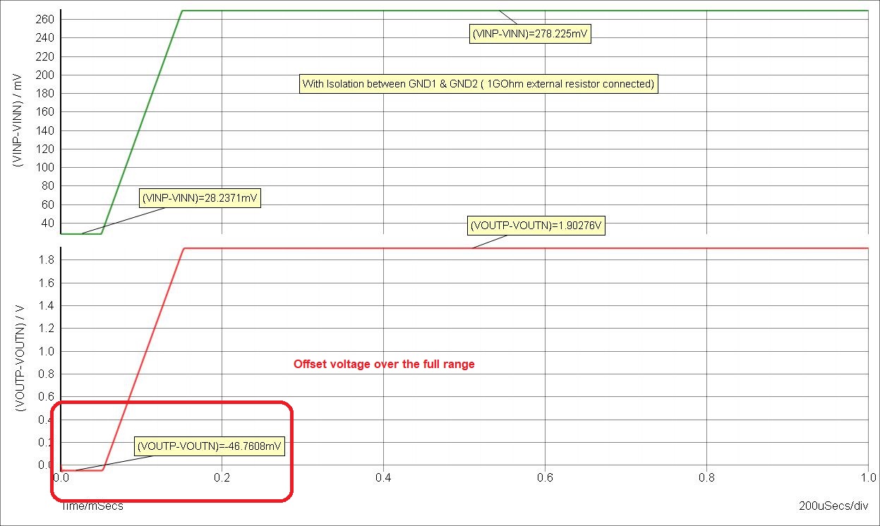
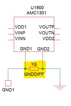
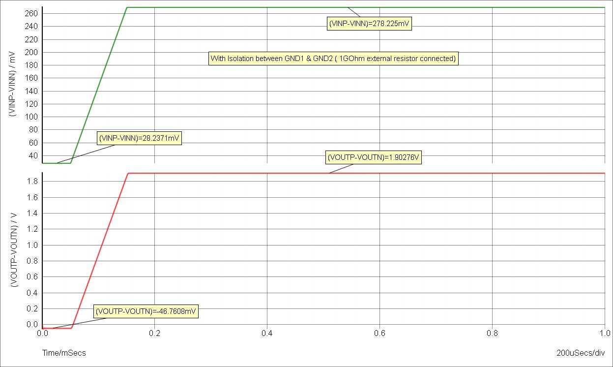
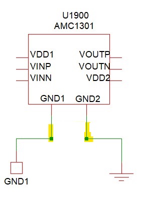
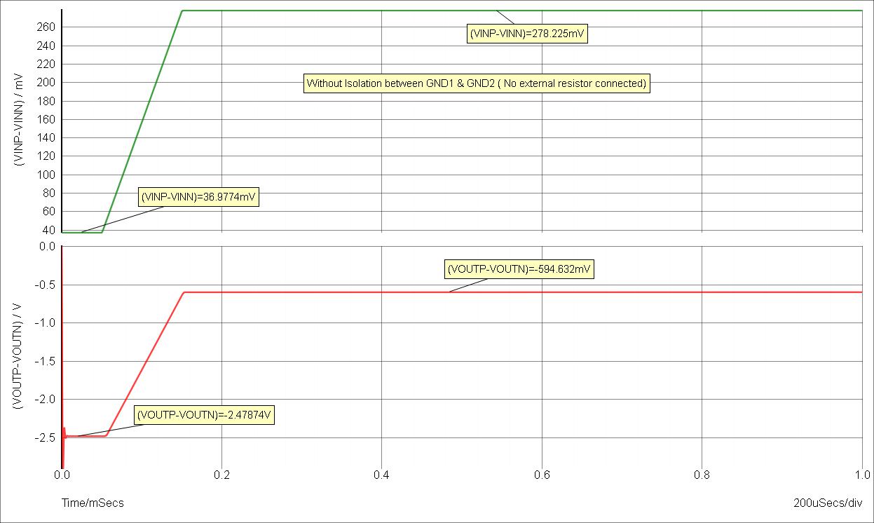
Case A: Above simulation is carried out with Different Ground (i.e., with isolation) for GND1 & GND2. This isolation is provided by placing a resistor of 1GOhms between GND1 & GND2 which is shown below. The result is shown below as per the Circuit diagram mentioned below.
Case B: Above simulation is carried out with Different Ground (i.e., with isolation) for GND1 & GND2. This isolation is provided with no resistor between GND1 & GND2 which is shown below. Since the spice code mentioned that it contains 100GOhms between GND1 & GND2. The result is shown below as per the Circuit diagram mentioned below.
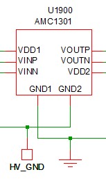
Case C: Above simulation is carried out with Ground Reversal (i.e., without isolation). GND2 is considered for High voltage side and GND1 is considered for Low voltage side. The result is shown below as per the Circuit diagram mentioned below.
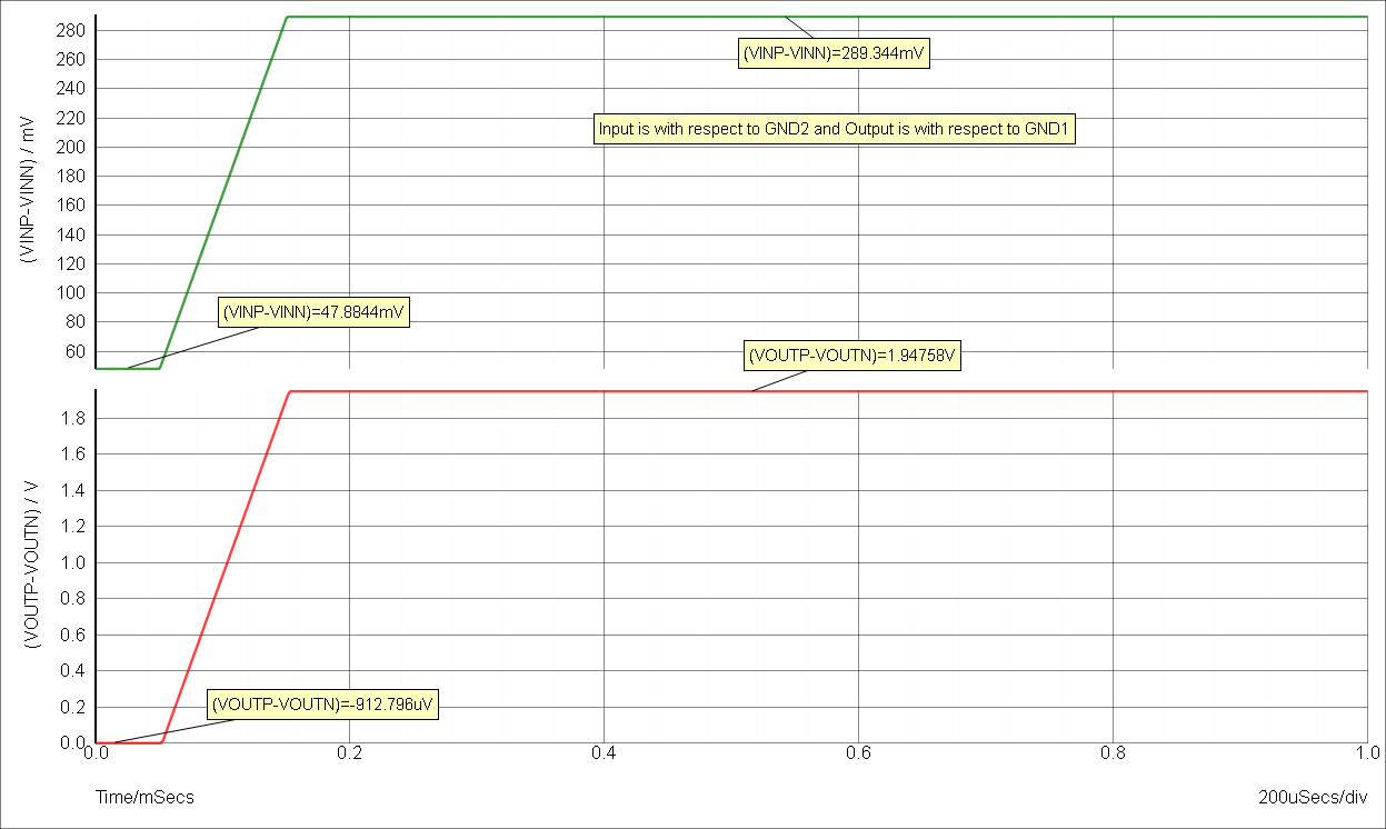
Query 1: Which case is correct while doing simulation? Both results vary, But if we observe "CASE A" output matches, Voltage across (INP - INN) = 278mV and Voltage across (VOUTP - VOUTN) = 1.9V which is almost gain of 7 times matches as per datasheet (G=8.2). While in "CASE B" is not matching i.e., without external Isolation resistor
Query 2: In "CASE A", when voltage across (VINP - VINN) = 28.22mV during t = 0 to 0.1ms, The output voltage (VOUTP - VOUTN) results with an offset voltage = -48mV . Is this simulation result correct or not? If correct, what will be the reason of offset voltage?
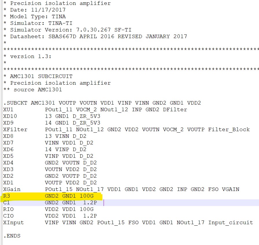
Query 3: As per spice model the resistance between GND1 & GND2 contains 100GOhms, If I place resistor of 1GOhm externally between GND1 & GND2 this makes an equivalent resistance of 0.99GOhms between GND1 & GND2. Is "Case A" is correct method to proceed?
Query 4: In "CASE C" (without external resistor considered i.e., 1GOhm connected between GND1 & GND2), the High Voltage side is considered w.r.t GND2 and Low Voltage is considered w.r.t GND1. The results are promising when compared to "CASE A" and "CASE B". Need to know, that "CASE C" schematic is correct or not?
Eagerly waiting for your response
Thanks & Regards
Athieshkumar T