This thread has been locked.

If you have a related question, please click the "Ask a related question" button in the top right corner. The newly created question will be automatically linked to this question.

OPA335: OPA335 Transimpedance Amplifier Circuit resulting in op-amp being damaged

Part Number: OPA335
Other Parts Discussed in Thread: ADS1248, TINA-TI

Hi Guys,

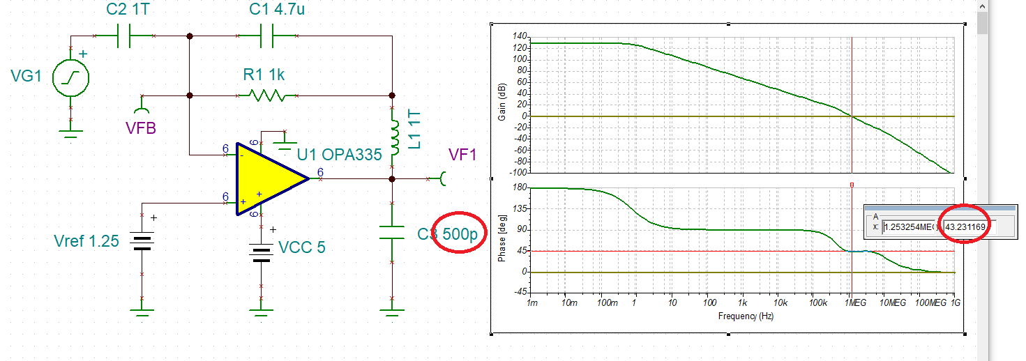
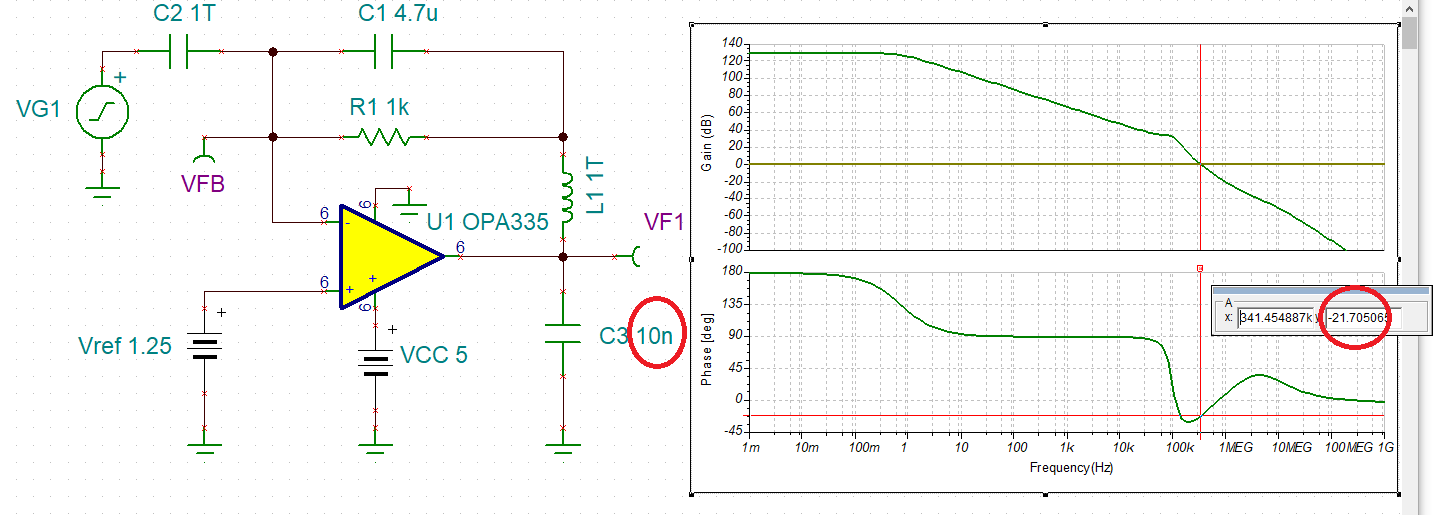
I have a peculiar issue I'm experiencing with a transimpedance amplifier circuit designed using an OPA335.The schematic is attached below,I have annotated it where possible to make the problem easier to digest.

The above circuit is being used as a transimpedance amplifier with a gain of 3300 set by the 3k3 resistor.The 4.7uF capacitor functions as a stabilization/feedback capacitor.The positive input of all the op-amps above share a common reference voltage i.e. a single MAX6070 IC provides a 1.25v reference for all 4 op-amps.The output of each of the op-amps is then fed to into 8 differential inputs of an ADS1248 ADC along with the 1.25v reference i.e. Output of op-amp to + differential input and 1.25v to negative differential input of ADS1248.

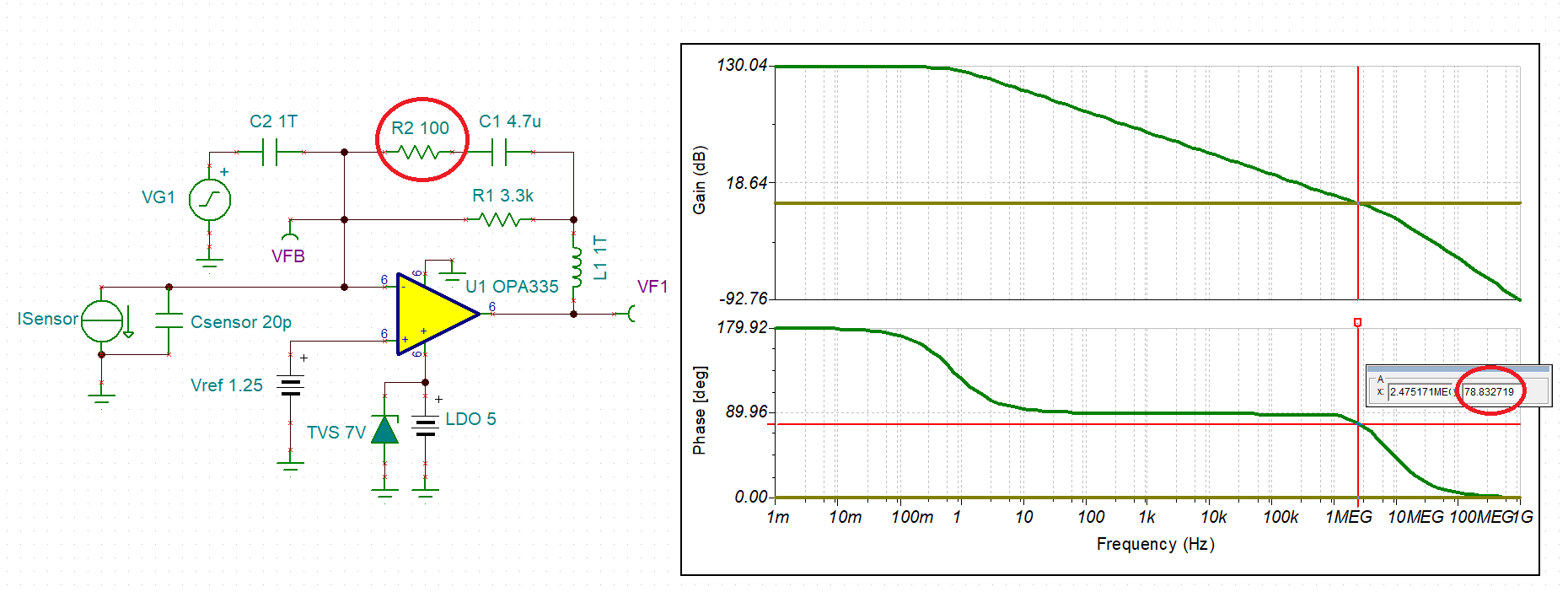
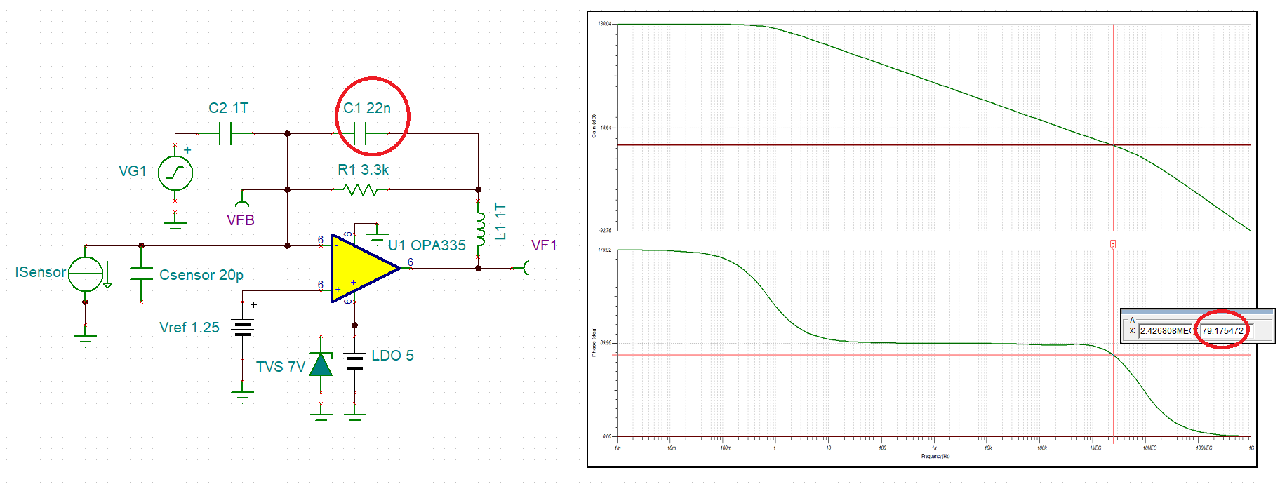
The above circuit is being used to amplify the signal generated by an electrochemical sensor used to measure breath alcohol levels.The sensor is connected across the MMBFJ177 JFETS,this is used to provide a virtual ground to allow the sensor to discharge when not in use.

After a few days of operation the OPA335 devices start failing,i.e. drawing current even when not in use and pulling the reference voltage down to 0.8v from 1.25v.I notice that after the fault occurs the OPA335 ICs show a low-impedance between Supply and GND pins.The same mode of failure has occured on 4 different PCBs.The 5v LDO on the schematic is powered from a regulated 12v supply.

Any assistance and general design advice/improvements to the above circuit would be greatly appreciated.

Kind Regards,

  • Hello Akshay

    One common culprit is you might be sitting there with each channel oscillating at much higher F than you are looking - dissipating a lot of power, raising the Tj and eventual failure. 

    Two missing pieces - your detector capacitance and as you go off the ADS1248, do you by chance put some big caps on that ADC at inputs - if so what value, 

    Here I estimated 20pF source C and 10nF load C, only 8deg phase margin, You feedback cap is huge, so I put in a self resonance of 4nH as a guess. This is a loop gain phase margin simulation. 

  • Hi Michael,

    There are no caps on the ADC inputs,it is being fed directly.

    The op-amp output to the + differential input of the ADS1248 and the reference fed into the - differential input of the ADS1248.

    Kind Regards,

  • Hi Michael,

    Just to confirm. What you are alluding to is that any further capacitive loading could be causing the phase margin to decrease to the point where the criteria for oscillation is met?

    Kind Regards,

  • Well you ask why are parts breaking after a few days, very unusual unless they are operating at very high Tj

    Have you checked to see if they are running very hot? 

    In the past, I have seen many failure mechanisms traceable to unperceived oscillations. 

    If the parts are not running hot, then there is likely something else going on perhaps related to overdrive

    What does your source impedance look like. 

  • Hi Akshay,

    the 4µ7 cap stores enough energy to destroy the OPA335 when abruptly powering down the circuit. As a remedy you could decrease this capacitance or insert a current limiting resistor which limits the current spike flowing through the OPAmp.

    Can you post the equivalent circuit model of your sensor so that we can carry out a phase stability analysis?

    Kai

  • Neglecting the sensor effect, the circuit is stable only with a capacitive load of up to 500pF while under 10nF load the circuit has a negative phase margin of -21 degrees (fully oscillates) – see below.  Thus, as Kai mentioned, in order to assure stable operation it would be critical to know the equivalent circuit model of your sensor as well as the filter used in front of ADS1248.

    Having said that, since the LDO is powered from 12V supply, it is quite feasibly that its reference output voltage may overshoot during power up above OPA335 absolute maximum rated supply voltage damaging the part. For this reason the circuit should be protected with 7V TVS on its supply pin – see below.

    Below please see Tina-TI schematic used for stability analysis. 

    OPA335 Akshay TIA.TSC

  • Hi Marek,

    We have added a 5v1 protection diode across the 5V LDO.I have attached the datasheet of the sensor in question herewith.I see in your simulation you are using a 1k resistor and not 3k3.There is unfortunately no equivalent circuit model in the datasheet. I am not using a front end filter. Connections are made directly to the ADC inputsBA-R-Sensor-Datasheet (1).pdf

    Kind Regards,

  • Hi Akshay,

    5.1V protection diode on supply pin may be too close to 5V LDO output and result in a large current flow.  Also, do you use a Zener or TVS on supply pin ?  A Zener may be too slow to clamp the LDO output overshoot below 7V absolute maximum required by OPA335. 

    With no LPF filter at the output, the circuit is pretty stable with 80 degrees phase margin - see below. 

    But 4.7uF in the feedback is very large and forms a low-pass allowing only very slow signal to be measured below 10Hz - do you really need it this low?  Also, as Kai mentioned, such a large cap stores enough energy that could damage the part during rapid shutdown.  Thus, you should either greatly decrease it (e.g. 4.7nF) or add a resistor, R2, to limit the current.  This hardly affects the stability of the circuit but will limit the current spike to less than 50mA thus preventing a potential damage – see below.

  • Hi Marek,

    I have changed the feedback capacitor to 22nF.

    Also,I meant to ask,is there anything wrong with feeding the same 1.25v reference used at the positive input of the op-amp to the negative differential input of the ADC?

    Kind Regards,

  • Adding 22nF feedback should be fine and eliminates the need for R1.  You do not show how you derive Vref but if it is a buffered reference voltage or series reference voltage, it is actually advisable to use it to drive both nodes, non-inverting input of the op amp and negative differential input of ADC, for higher precision.

    Attached please find Tina_TI schematic you may use for your further analysis.

    OPA335 Akshay TIA AC.TSC