This thread has been locked.

If you have a related question, please click the "Ask a related question" button in the top right corner. The newly created question will be automatically linked to this question.

ACF2101: Keeping Other Currents out of Photodiode Integrator Return

Part Number: ACF2101

I am trying to use AC2101 to detect very tiny currents using integration times in the 20-second range.  So I’m trying to minimize any ground currents finding their way into the signal path. 

What is the purpose of the Select switch that connects input return pin another pin (output return)?


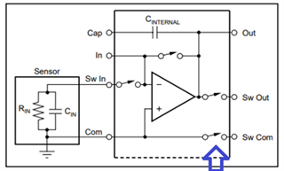
Where is the best place to connect the photodiode return (the net between cathode to COM) to ground?


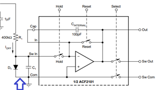
Is COM A connected to GND A inside the part?  Do those pins need to be connected together close to the part to prevent currents from flowing between them?  

  • Hi Charles,

    Here is what the ACF2102 datasheet states about the Select switches, "The two Select switches can be used to multiplex the outputs when multiple integrators are connected to a common bus. Figure 5 shows a number of ACF2101s multiplexed together into an A/D converter."

    Figure 5 shows the output and the common Select switches driving the inputs of an instrumentation amplifier. Depending on the design of the instrumentation amplifier its performance may be degraded if the source impedances are not close. By including an additional switch in the common line both the output and common include the ON resistance of the analog switches. This provides a closer impedance between SW Out and SW Com match looking back into the two pins.

    It is best to try and minimize the trace lengths to the photodiode in an effort to minimize the support of leakage currents. Therefore, the photodiode should use traces connected as direct as possible to the SW In and Com pins on the ACF2101 input side.

    The datasheet doesn't really say anything about the GND A and GND B pins other than in Fig. 1 it states "These points must be connected to a common ground point, or a ground plane." It shows the Com and GND pins with a common ground symbol in the figures. Because of this statement it is highly likely the these pins are connect together internally.

    Usually, the hardest part of taming leakage currents on an extremely low input current amplifier product is PC board cleanliness. If you are using solder with water soluble flux, we recommend after the general board cleaning that it be subjected to two, separate cycles of ultrasonic cleaning in DI water. The board needs to be fully dried after each ultrasonic cleaning. The ACF2101 performance can be astonishingly good when applied with a very clean PC board.

    Regards, Thomas

    Precision Amplifiers Applications Engineering