This thread has been locked.
If you have a related question, please click the "Ask a related question" button in the top right corner. The newly created question will be automatically linked to this question.
Dear Team,
I am using LM7171 as a clock distributor in my circuit. It is working at +15V and -15V the output from this Opamp is going to the clock input pin of my ASIC.
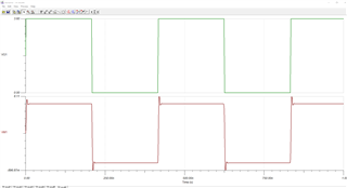
when the clock amplitude is 3.6V ,I am seeing a glitching at the output.I/P CLK frequency is 2.4Mhz
May I know where I went wrong. Please find the attached TINA simulation file.
Regards
HARI
Morning Hari,
Well you have a 1nsec input edge, that is likely putting the LM7171 into slew limiting which will cause that overshoot,
Well it is not letting me insert the snip, but if you slow the edge down in sim (or with an RC circuit into the V+ input), the overshoot should go away.
try again, I was not logged in,
here is a 5nsec transition - notice the overshoot is gone
Hi Mic,
Good day to you Mic
I put a capacitor of value 1.5pF across the feedback resistor and glitches were gone. I did it via trial and error.
Could you please tell me how to calculate the compensation capacitor value using maths.
Regards
HARI
I actually do not prefer the feedback cap as that shapes the noise gain to 1 at higher F sometimes moving to a lower phase margin condition, a simple RC into the input V+ pin is what I prefer. And essentially, once you have a small signal frequency response, you are trying to assess if the peak dV/dT on the output might exceed the available slew rate for whatever part you are using. And, you might want to consider a current feedback solution as they naturally have much higher slew rate.
Interesting could you please tell me more about this "a simple RC into the input V+ pin is what I prefer.",with some circuit diagram.
Or you can tell some reference so that I can read.
My Clock is coming from a function generator with output impedance set to 50ohm. This CLK amplitude is first made half then amplified to make the input value.
Will this RC network causes any issues.
May I know how to design the RC network
Dear MIC and Kai
I did not understand anything about this statement. I am very much interested in analog circuits. Trying to learn more.Could you please expalin the below ords from Mic.
" And essentially, once you have a small signal frequency response, you are trying to assess if the peak dV/dT on the output might exceed the available slew rate for whatever part you are using. And, you might want to consider a current feedback solution as they naturally have much higher slew rate"
Regards
HARI
Hi Hari,
To put it simply, the 'peak dV/dt' is the maximum change in voltage with respect to time, or the 'slope' of the voltage signal. The slew rate is just what we call this when talking about what the amplifier is capable of delivering. If you need the output to change faster, (larger slope/slew) then you could choose a part with a faster response (higher slew rate). Current feedback amplifiers are an option, although they can potentially be trickier to implement if you are not familiar with their characteristics. The solution presented here, the 'RC' network, is simply a low-pass filter that will limit the input slope so that it does not exceed what the amplifier can deliver. This is also sometimes called increasing the rise-time or the time constant of the input signal. For a more in-depth look at this issue and why exceeding the available slew rate will cause the device to behave undesirably, please see TI Precision Labs - Op Amps: Slew Rate Introduction | TI.com Video
And for a considerably more in depth look,
This maps a 2nd order response to a peak dV/dT
https://www.edn.com/what-is-op-amp-slew-rate-in-a-slew-enhanced-world-part-1/
And part 2 gives a nice estimating equation with some examples,
Then later I did this article also on issues arising from slew limiting
And part 2,
This is way more than you need for passing a clock around - you might also consider the output interface, if you are driving an ASIC, your really only need a small series R to isolate its input C, not that 50ohm shunt if you are not driving through a cable.
Thanks Mic..I will go through this and will contact you for clarifications.
We are driving the clock through an SMA cable. The clock is coming from a function generator. This clock will be given to 4 ASICs present in the ASIC Evaluation board .
Dear Team,
I was checking the datasheet of LM7171 in page no 19 I saw circuit called Compensation For Input Capacitance ,they have given an equation for feedback capacitor ,I have 2 questions regarding it.
1)May I know how they arrived the equation
2)Same equation is applicable for Non inverting configuration also.
Please reply
Regards
Hari
Hi Hari,
That equation describes the dominant pole stability condition for the compensation capacitor. Essentially the RC time constant for the pole you are introducing should be larger than the RC time constant caused by the input capacitance. This applies to non-inverting configurations as well.
If you are interested in loop gain transfer functions and op-amp stability, we have several trainings available that you might enjoy. I would start with TI Precision Labs - Op Amps: Stability - Introduction | TI.com Video and the video that follows, TI Precision Labs - Op Amps: Stability - Phase margin | TI.com Video
Best,
Sam