This thread has been locked.

If you have a related question, please click the "Ask a related question" button in the top right corner. The newly created question will be automatically linked to this question.

LMC6035: Output oscillation on LMC6035 with DC input and 1K load

Part Number: LMC6035

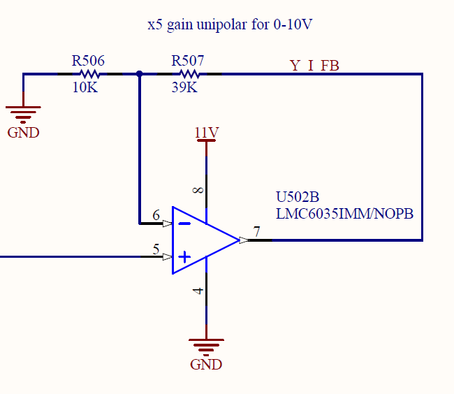
I am trying to utilize the LMC6035 as a non-inverting gain amplifier. I have the circuit seen below (bypass cap present in design but not shown). I have a stable 1V DC signal on pin 5 of the LMC6035, and I want a stable 5V output signal on pin 7 (i.e. net Y_I_FB). I am attempting to drive a simple resistive load, but I am getting large oscillations on the output. With the 1V input, and a 1K load resistor I am getting an output oscillation of 1V-5V at ~425 kHz

  • Hi Carlton,

    I would mount a 10pF cap across R507. Also, consider to decrease the values of R506 and R507.

    Have you connected a 100n bypass capacitor from pin 8 to pin 4 of LMC6035?

    Is there any capacitive load at the output of LMC6035? If so, mount an isolation resistor of 47...100R directly at the output. Keep in mind that voltmeters and scope probes can show considerable capacitances.

    Mount R506 and R507 very close to the LMC6035 to avoid stray capacitances and inductive loops.

    Use low pass filtering at the +input of LMC6035, if the input signal of LMC6035 is remoted.

    Kai

  • Thanks for the suggestions!

    I do have a 100n bypass on pins 8 and 4 (as noted in my original post). R506 and R507 are right next to the op amp. The + input signal is an output from a nearby instrumentation amp that is DC stable (only a couple mV peak to peak, nothing which should be causing a 4V oscillation on the output).

    I'll try the cap across R507 and see if that helps, but if not I'll probably just change amps as that will not require a board respin.
  • Hi Carlton,

    I don't think that it has to do with the LMC6035. The circuit is deadly simple and should work beautifully. I think the issues have to to with your setup, cable lengths, stray capacitances, the absence of shielding, and so on.

    Kai

  • The reason I wanted to switch is actually that I'd be going back to an old op amp. In the first spin of this board I used a similar design with a different op amp (trace lengths were actually slightly longer due to the old op amp being a SOIC package and the LMC6035 I'm using is in a VSSOP package). I didn't have any issues with that, so I'll most likely swap back since it seems to handle the parasitic capacitance better.

    With the addition of your suggested compensation circuitry as well, the design should be even more robust. I'm not sure where I could begin looking for parasitic capacitances on the board layout itself though as there's nothing nearby and the traces are fairly short and thin. Perhaps on the next spin I'll change the dielectric size between my top layer and power planes to help with that as well.