This thread has been locked.

If you have a related question, please click the "Ask a related question" button in the top right corner. The newly created question will be automatically linked to this question.

INA202: about high Vout and CMPin voltage when load supply ramps up

Part Number: INA202

Hi Dear expert,

My customer uses INA202 to detect Power amplifier current. They found some parts during load supply(PA supply) ramps up to 48V, when it reaches to 0.5V, CMPin will reach to 0.6V and CMPout will become high and falsely power down PA. 

Below is the schematic: 

In customer's application, Rshunt=10ohm, R1=18.7kohm, R2=6.5Kohm.

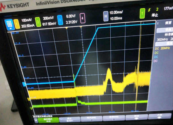
Below is the load supply and Cmpin wave form:

Blue line is the load supply, starting from 0V to 48V. When it reaches to around 0.5V, green line is the CMpin voltage, it will reach to 0.6V. and it will trigger PA protection, and will shut down PA supply.

We have done several tests:

1. During PA supply voltage ramps up to 0.5V, some parts CMPin voltage will reach to 0.6V, while some parts will reach to 0.3V. if CMPin reaches to 0.6V, it will falsely trigger PA protection. i calculate the current, 0.6V CMPin means Vsense=24mV, Shunt current=2.4A. While in normal PA working condition, current=1.7A.

2. Customer tried to short Vin+ and Vin-. But still observe CMPin voltage reaches to 0.6V in bad parts when load supply reaches to 0.5V.

Support needs:

1. Can you please review the schematic and check whether Rshunt is proper?

2. Can you please reproduce this on demo board to see when load supply is 0.5V, whether CMPin will become 0.6V or some voltage level?

Thanks very much for your reply.

Joyce


  • Hello Joyce,

    Thanks for reaching out on the forum.  I think your customer's issue might be related to the issues found in the posts here and here.  As such, adding an RC low pass filter to your RESET pin might help.   As for the shunt value, that seems fine.  After your customer attempts using a filter on the reset pin, if the part still does not work we can look into trying to reproduce your customer's test conditions.  However, we will need more details on how your customer is powering on the device and how they are cutting power to the device.

  • Hi Patrick,

    I am afraid the two cases are not same as my case.

    My case is not related to REset pin and customer does design RC filter for RESET pin.

    My case is related to high output voltage of the amplifier when the common mode voltage of Vin+ and Vin- is around 0.5V. Please check the scope snapshot, blue line is the load supply power, green line is CMPin, when the load supply ramps to 0.5V, the CMPin will reach to 0.6V, which means the output of amplifier reaches to 2.4V when load supply is 0.5V. When load supply continues to ramp up, the cmpin voltage will become normal.

    They also tried to short Vin+ and Vin-, making differential input=0V, while the load supply ramps to 0.5V, customer still observes high output voltage of the amplifier. it means this issue is related to common mode voltage is 0.5V, differential voltage=0V, the output is very high.

    Please try to reproduce this on demo board to help us identify the problem. thanks a lot!

  • Hello Joyce,

    Sorry for my misunderstanding.  I do not have INA202 samples right now, but I should have them tomorrow and will be able to test in the lab then.  When the customer's common mode is ramping, is their INA202 supply line also ramping or is it already stable at 5V?

  • Hi Patrick,

    Yes, INA202 supply is stable at 5V. 

    Joyce

  • Hello Joyce,

    I ran some tests in the lab and I do see the same behavior your customer is seeing.  At the moment I am trying come up with a workaround to suppress that glitch.  I will try to get you some proposed fix by tomorrow.

  • Hi Patrick,

    Good to know the demo board can see the similar phenomenon. will wait for your update. :) 

    Thanks a lot for your support!

    BR,

    Joyce

  • Hello Joyce,

    I found a workaround for suppressing the glitch. It utilizes device VCC and the VCM as control signals for when CMPIN is pulled low.  VCC goes directly to one input of the AND gate.  The other gate input is a little more complicated.  As the VCM ramps, the voltage divider consisting of R5 and R9 is initially off.  Once the VCM exceeds the zener reverse breakdown voltage, the voltage divider turns on.  You will need to choose the zener and divider based on the lowest VCM your customer wants to use.  The next zener prevents the divider output voltage from exceeding 5V.  I include this in case you want to use an AND gate that has input requirement that may be lower than the divider output without the zener.  When both AND_VCM_IN and AND_VCC_IN are low the internal open drain output mosfet of the AND GATE is turned on creating a shunt to gnd, thereby suppressing the glitch (Assuming the RDSon is really small).  Once both AND gate inputs are high, the SHUNT2GND_Control signal goes low thereby turning T3 off.  Some leakage current will pass through R3 and will need to be accounted for.  Below is my implementation along with the TINA circuit.  While this circuit illustrates a way to suppress this glitch, your customer may want to determine if better FETs and diodes can be used as I simply used the parts available in the default TINA library. 

    /cfs-file/__key/communityserver-discussions-components-files/14/GlitchWorkaround.TSC

  • Hi Patrick,

    Thanks a lot for your effort on the work around solution. The workaround basically focused on the CMPin circuit.

    Customer wants to know the root cause of Vout reaches to 2.4V while Vin and Vout Common mode voltage is around 0.5V? Can you please explain this? They need to be fully clear about the root cause before implementing any workaround solution. 

    "My case is related to high output voltage of the amplifier when the common mode voltage of Vin+ and Vin- is around 0.5V. Please check the scope snapshot, blue line is the load supply power, green line is CMPin, when the load supply ramps to 0.5V, the CMPin will reach to 0.6V, which means the output of amplifier reaches to 2.4V when load supply is 0.5V. When load supply continues to ramp up, the cmpin voltage will become normal."

    Thanks very much for your support.

  • Hello Joyce,

    This actually can be found in the datasheet. The explanation is provided on page 20 section 7.4.2.4.

  • Hi Patrick,

    I checked the datasheet 7.4.2.4 low Vsense case2. Customer test result is similar to datasheet description. However, there is some difference.


    1. In datasheet, it describes Vout test limit for INA202 is 2V. My customer tested result is 2.4V. It exceeds the test limit. They also tested some normal parts, the CMPin is 0.3V, i.e. The Vout is 1.8V. This is normal. Why some parts Vout exceeds to 2.4V? Is this bad part that failed to be screened out?

    In customer's application, Rshunt=10 mohm, R1=18.7kohm, R2=6.5Kohm.

             2.  you mentioned you also reproduce this phenomenon, I wonder how much is the Vout voltage?

    Thanks a lot for your reply in advance.

     Joyce

  • Hey Joyce,

    Although we covered some of this over email, I will also post here to the benefit of any other forum user encountering the same issue.   Also I do have some updates to the prior responses I gave,

    1. Parts that exceed specifications in the electrical characteristics table should be screened out.  Turns out there is a section on page 6 that does specify a max limit for Vout when vsense is less than 20mV.  It is 2V like you said.  However, after consulting with a colleague this spec appears to be a DC specification that was likely taken after some settling time.  Therefore if overshoot is considered, its possible that Vout could be greater than 2V.

    The difference in behavior among your devices could be attributed to manufacturing tolerances.

    2.  For my test, the output went to roughly ~1V with CMPIN voltage at ~250mV.  Since, performing that test I have done a few additonal tests.  My key observations were that below 20mV Vsense on my device, the glitch was not always large.  Typically the largest glitch was found below 10mV.  I also noticed that changing the VCC potential had an impact on the size of the glitch.  Lower supply voltages typically had bigger glitches.  From this behavior I suspect that if your supply droops at all during the VCM ramp up, the affect may be even more pronounced.  The other key item I noticed was that a faster VCM ramp up yield a significantly smaller glitch.  This probably due to the device leaving the worst operating region more quickly.

  • Hey Joyce,

    To consolidate where the responses are I will close this thread for now and continue to support you through email.

  • Hi Patrick,

    Agreed. Thanks a lot for your support!

    BR,

    Joyce.