This thread has been locked.

If you have a related question, please click the "Ask a related question" button in the top right corner. The newly created question will be automatically linked to this question.

The output voltage of this chip using rcv420 is 1-6V instead of 0-5V

Other Parts Discussed in Thread: RCV420, XTR111

I designed this circuit according to the instructions in the data sheet (1 pin in the circuit is not soldered to the board and has been left floating), but its output is a voltage of 1-6V instead of the 0-5V originally expected Voltage value. As for the input, I used the XTR11 chip design circuit to output a 4-20ma current, which is accurate after the oscilloscope test. I don't know where the problem lies. Please help me to see what the problem is, thank you very much!

  • Hi ,

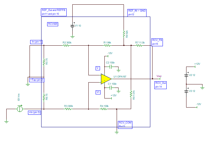
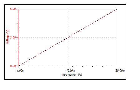
    The RCV420 configuration appears to be correct accepting a 4-20mA input and generating a 0-5V input.  Below is an approximate SPICE simulation using a behavioral/approximate circuit based on the datasheet diagram.  

    However, it is not clear how the 4-20mA input signal is connected on the schematic. The schematic appears to show a capacitor at the IN+ input and you have mentioned you use an oscilloscope to measure the 4-20mA current.  Is this an AC or DC input signal?  Which XTR11 device are you using to generate the 4-20mA signal?  If this an AC signal, what is the frequency? How do you measure this input current using the oscilloscope?  Can you please show the complete schematic or diagram showing the transmitter circuit and how the input signal is connected?

    Thank you

    Luis

  • Hello, dear engineer,

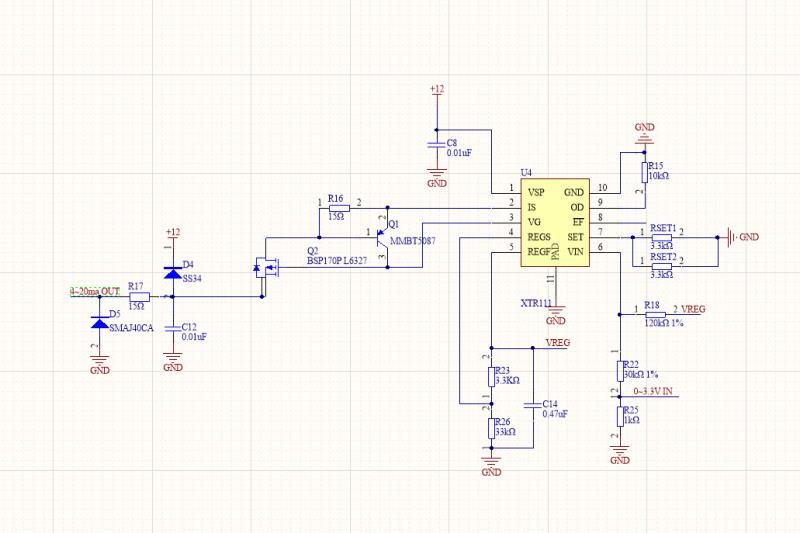
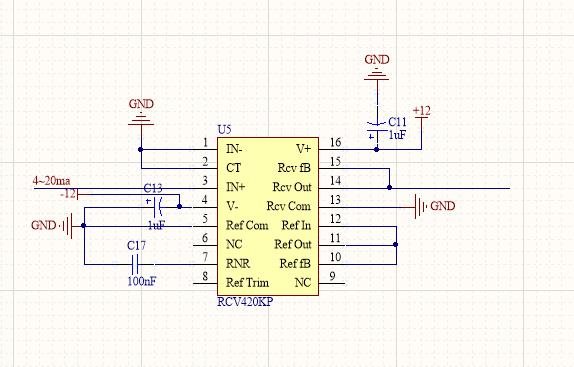
    The first picture is a circuit diagram that generates 4-20ma, and the second picture is a circuit diagram that receives 4-20ma current and converts it to 0-5V voltage, although the output is not the ideal voltage.

    In the third picture, signal 1 is a voltage signal of 0-3.3V with a frequency of 1.5HZ generated by the signal generator. This voltage signal is the input of the first picture. Signal 2 is the voltage signal of RCV420 input pin.

    In the fourth picture, signal 2 is the output voltage of RCV420. The output voltage is not 0-5V originally desired, but is raised by about 1V as a whole.

    These are the current situations. Thank you for helping me to see where the problem lies. If you need anything else, please send me a message, thank you!

  • Hi ,

    On the XTR111 circuit, the drain of the PFET should be connected to the load (RCV420), and the source should be connected to IS pin (2) through resistor R16. The schematic on the post show these connections reversed.  Please check the PFET transistor connections (refer to datasheet schematic below).

    - In regards to the RCV420 circuit, the only way I can reproduce the issue where Vout = 1-V to 6-V is if I purposely leave RCV420 REFIN (12) is left floating.  Can you also confirm that REFIN is connected to the +10-V reference, in other words, please confirm that pin 10, pin11 and pin 12 all measure +10V with external meter.

    - Is this occurring in one PCB or several?  If possible, please share the PCB layout as well. 

    Thank you and Regards,

    Luis

  • Dear Engineer.

    I'm very sorry to reply to you so late.In the XTR111 circuit part, I checked it and found that the PFET was indeed reversed. However, this part of the circuit can output 4-20ma when the input voltage is 0-3.3V. I'm very surprised about this. I will modify it in the next board.

    Regarding the circuit part of RCV420, the following figure is its PCB part. The 3rd pin is a signal input, and the 14th pin is a signal output. This looks really simple. I checked the voltages of pins 12, 11, and 10 with an oscilloscope as you said, and the results showed that they were about 2V. To avoid the problem with the chip, I re-soldered another circuit board, and the result was the same as the previous one. These three pins did not reach the 10V reference voltage on the data sheet. So what do I do? Is something wrong with the circuit? Or should I connect another 10V to these three pins?

    This is my first time designing a circuit and drawing a PCB. Thank you very much for your patience.

  • Hi ,

    Thank you for the information,

    The layout above does not show clearly the GND connections.  For example, pin 1 of C13 is labeled GND, however there is no via or trace showing the ground connections. Is there a GND layer underneath the device?  How are you connecting the GND net on the PCB board?

    Please post the complete schematic of the RCV420, and the corresponding PCB layout including all layers so we may review. 

    Thank you and Regards,

    Luis

  • Dear Engineer,

    Thanks for your patience.The following file is the schematic and PCB of my entire circuit board. The lower left corner is the schematic diagram of the RCV420. In the test, I only used the part in the black box, and did not use the voltage division part behind. The t1-t9 in the figure are the test points I used in the test and do not represent resistance or capacitance. Sorry for the inconvenience.

    board.rar

  • Hi ,

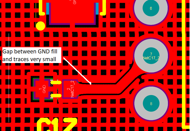
    Looking at the layout, it appears there is no sufficient clearance/gap between the GND fill and the signal traces and component pads. I suspect some of these connections could get shorted to GND. 

    For example, NetC17_2, shows only a ~2 mil gap between the GND fill and the trace.  It may be possible that these signal traces and component pads are getting shorted to GND when manufacturing the board or soldering the components.  Most PCB fabrication processes require this gap to be much larger, typically around  ~8 mils or ~10 mils minimum.  Since there is room on the PCB, you could set this clearance to be much larger and avoid this issue (or you may need to consult with your PCB manufacturer as to what is the minimum clearance requirement).

    Regards,

    Luis

  • Hi,

    we use a clearance of 0.3mm for reflow soldering and 0.35mm for hand soldering of connectors.

    Kai

  • Dear engineer, 
    I'm very sorry to reply to you so late. Thank you very much for your suggestions, I will modify it in the next board.
    Thanks again for your patience!

  • Dear Engineer,
    Sorry to bother you again. Can I consult you again if something goes wrong later?

  • Hi,

    of course you can :-)

    Good luck!

    Kai

  • Hi,

    Yes, feel free to post a new question.  If this post is closed, please feel free to open a new post query.

    Also, let us know if you want us to review the revised Altium schematic/layout prior ordering the new boards.

    Thank you and Regards,

    Luis