This thread has been locked.

If you have a related question, please click the "Ask a related question" button in the top right corner. The newly created question will be automatically linked to this question.

INA818: Considerations for the input/output filter.

Part Number: INA818
Other Parts Discussed in Thread: INA118

Hello again!

I am currently designing a circuit in which to adapt the measurement of a gauge to an ADC.
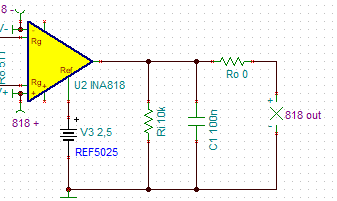
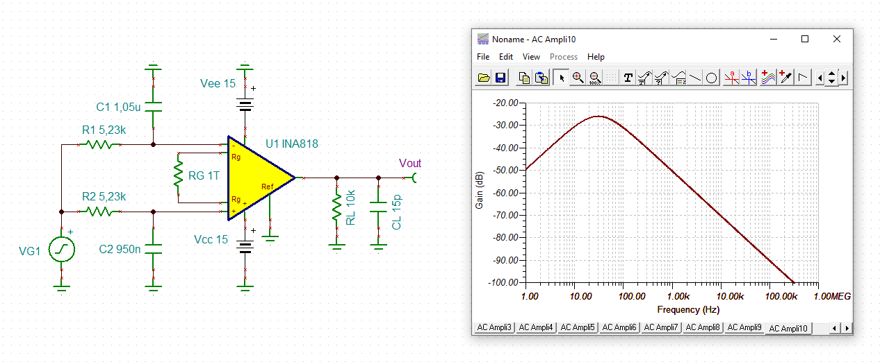
As I have already commented in other threads regarding the use of the INA818, I have considered a satisfactory output but I have not yet included any RC parallel differential or input filters.

1.- For the differential input filter for this specific device and application, I will use the TI tool, Analog Engineer's Calculator -> "INA Vcm + Dif filter"
The help of the tool itself is really good, but I still need to know what frequency range to design.
How do I know which one I should consider?
And how do I make sure that by putting a resistor in series with the Wheatstone bridge connection I am not going to modify the reading?

2.- In the case of the output filter, a parallel RC is normally recommended looking for the stability of the amplifier.
What specific INA818 criteria and data should you take to make it as beneficial as possible?

I have used this documentation as a reference http://www.ti.com/lit/pdf/tidub00 and the great help of this professional forum

Thanks!

Regards.

3225.INA818_INA118_ReferenceDesign-TA_SIM.TSC

  • Hi SrgiO,

    what is your signal frequency range? The datasheet of gauge often specifies the bandwidth and settling time.

    And the datasheet of ADC usually specifies the component values of necessary charge kickback filter.

    Kai

  • Thank you Kai!

    Hi SrgiO,

    Happy to help. In addition to Kai's questions, can you also provide the gauge and ADC part number?

  • Hi Tamara and Kai, thank you both very much.

    I don't have any defined, I mean the theoretical aspects to be able to apply to any gauge and ADC.

    If you wish, we can propose an example, but I can't find the data that Kai asks for. I've been looking at HBM, RS Pro, Omega .... and the gauge's frequency range is not mentioned in the datasheets. The measurements are in DC according to the scheme that I proposed.

    For the ADC, I was thinking of using an MSP430 Launchpad or Arduino, for example. But once again, I do not know what aspects are influencing, in this case, for the INA output RC filter.

    Thank you!

  • In order to better position ourselves, I add the following screenshots.

    This is specifically the configuration at the exit of the INA proposed in the schematic included in the tidub00 documentation from Texas.
    It's really necessary? Why these values and not others? How to adapt it to each INA and ADC?

    In other schematics I have found that the resistance in series with the output is put after the RC parallel. Is it similar to the previous one? Does it change something?

    Thank you!

  • Hi SrgiO,

    Ri stands for a typical load.

    C1 in parallel to Ri is a no-go. 100nF is far too much load capacitance to be directly connected to the output of INA818. If you intend to connect a capacitive load, then do it as shown in the upper scheme with an isolation resistor of R8 = 47...100R or more, if the circuit allows.

    By the way, do you know this appnote?

    slaa045.pdf

    Kai

  • Thank you for sharing that app note, Kai!

    Hi SrgiO,

    Kai is correct. Ri is just the typical load. I would not recommend hanging a large capacitor off the output like that, unless there is an isolation resistor. A large capacitor at the output may lead to significant stability issues. Have you seen our TI Precision Labs training videos on op amps? We have a chapter on stability: https://training.ti.com/ti-precision-labs-op-amps-stability-introduction?context=1139747-1139745-14685-1138805-13848

  • Hi Tamara and Kai,
    I have been the time that I have been able to see the interesting information that you have sent me.
    Once again I thank you for helping me to increase my electronic knowledge. It is very good information!

    So any resistive or capacitive load suppose a risk to stability or loss of precision.
    Is Ri then a load that imposes the ADC?
    that is, Ri is not a resistance that must be "soldered" at the INA exit, is it? Therefore, is it better not to put any component if it is going to be connected to an ADC?

    Thank you!

  • Hi SrgiO,

    Some ADCs may require an input filter, here is a circuit example with explanation: http://www.ti.com/lit/an/sbaa282a/sbaa282a.pdf?&ts=1589839598711

  • Hi SrgiO,

    I think you can omit the charge kick back filter. Just use a simple isolation resistor, R8 = 100R...220R:

    Kai

  • Thanks for sharing, Kai!

  • Woohoo!

    First of all, thank you very much for the responses. For real! It feels like I'm learning a lot more here than when I was in college. :-)

    1.- Firstly: "I think you can omit the charge kick back filter."
    Is this statement due to the fact that the kick-back circuit can be neglected because the setup time of the INA (12 - 60) us is equal to or slower than the maximum ADC speed of the MSP430C32x (12us at 1MHz)? Or is it for another reason?

    2.- "Just use a simple isolation resistor, R8 = 100R ... 220R"
    Based on the equation, wouldn't it be even better not to connect any R8? Since R8 + 2k must be as small as possible ... well... better than R8 = 0, right? 

    3.- The data in the INA818 table is taken with an RL = 10k. Is it therefore necessary that I mount an RL = 10k on my circuit or is it better not to put it? Connecting the INA output directly to the ADC of the MSP, for example.

    I am sorry if it sounds strange, or very silly, but it is that sometimes I do not understand when a resistance (R8 or RI In my first capture of previous schematics) is in the circuits "simulating a load" or it is really an essential component for it to work properly.

    Many thanks.

    I await your interesting responses!

    Cheers!

  • Hi Srgio,

    I would choose R8 = 100R and an ADCLK of let's say 500kHz. This gives you a sampling time of 24µs. 12µs will the INA818 need to settle to 0.01% and the remaining 12µs allows the "2.1k + 42p" RC-network to fully charge up.

    There's no need to mount a resistor from the output of signal ground.

    An isolation resistor in SERIES to the output IS necessary, if a relevant load capacitance needs be connected from the output to signal ground. But there's no need to mount a resistor from the output of signal ground. The only reason why a load resistance of 10k or 2k or else is given in the datasheet specifications or is "mounted" in the simulation is that the output voltage swing of OPAmp and some other performance data depend on the amount of this load resistance. For instance, no OPAmp can drive arbitrarily small load impedances. This would mean infinitely high output currents. See also figure 37 and 38 of datasheet.

    Kai   

  • Thanks, Kai!

    Hi SrgiO, let us know if this is resolved for you :)

  • Hi Kai and Tamara,
    I'm sorry for the delay in answering. Believe me that I would have liked to answer you as soon as possible, but I have had different duties to attend to. Thank you very much for staying tuned.

    Indeed Kai, the insulation resistance of 100 Ohm seems the ideal to put it on. I think that for this part, you have helped me to see it and I already have it clear.
    On the other hand, it makes me put myself in the worst case:
    Where settling time is 60us for 1000 Gain.
    So in this case, with the same Rlim = 100Ohm it will give "2.1k + 42p" equally but now the ADCLK must be configured to be something more than 60us.

    How much more will it be correct? Double at least?
    120us => ADCLK = 100khz, right?

    Once this is defined....I return to the subject of the differential input filter.... There is less left, that's good! :D
    In one of the texas application notes the cutoff frequency is set at 15khz and the common frequency at 305kHz .... What or where are these values ​​regulated, why not others?


    Thank you!!! I am really very happy on the day I decided to participate in the forum.

    Cheers!

  • Hi SrgiO,

    an ADCLK of 125kHz results in 96µs. This should be sufficient.

    I will later respond to the input filter question.

    Kai

  • Hi SrgiO,

    the INA818 shows a very good rejection of common mode noise (see also figure 17 of datasheet):

    sergio_ina818_1.TSC

    Additional common mode filtering can drastically improve the overall common mode rejection:

    Unfortunately, in reality unavoidable manufacturing tolerances and drifts (!) of filter components can neutralize this advantage. See the result with +/-5% toleranced 1nF filtering caps:

    Manufacturing tolerances and drifts of filtering parts can even totally ruin the common mode rejection. See the simulation with +/-5% toleranced 1µF filtering caps:

    While there's an improvement at very high frequencies, the common mode rejection at low frequencies is totally eroded.

    Because of all this a rather high corner frequency of common mode low pass filter should be choosen. This prevents the common mode rejection from being degraded all too much at lower frequencies by manfufacturing tolerances of filtering elements, but still helps to suppress nasty HF EMI which can result in unwanted demodulation effects.

    In opposite to this common mode low pass filtering, differential low pass filtering has no direct effect on the common mode rejection. This allows the use of a much lower corner frequency for the differential low pass filter.

    Kai

  • Excellent answer as always Kai!
    Thank you!

    The functionality and design criteria for the input filter have now become very clear to me.

    Now it remains to know one of the questions that I have always had ...

    What is the typical design frequency to avoid FH EMIs?
    Does it affect the same frequency in differential as in single-ended?

    Thank you!

  • Hi SrgiO,

    there's no simple answer. In fact it depends on many factors like bandwidth of INA, bridge resistance, imbalance of bridge, frequency spectrum and level of EMI, acceptable increase of noise, etc.

    A good starting point is when your common mode filtering provides about 10...20dB dampening at the unity gain frequency of INA. Use very narrow tolerated filter components like +/-1% toleranced low drift caps (e.g. NP0) and +/-0.1% toleranced low drift thin film resistors. Keep in mind that the imbalance of bridge can totally ruin the balance of filter resistors! If your bridge imbalance is 100R and you take 1k filter resistors, then the effective resistor tolerance is awful 10%...

    Kai 

  • Hi!
    How's it going? I hope well with all of the pandemic ...

    Well, I understand that it is difficult to give answers that are always valid for all circuits.
    When I ask, I really look for "ways" or "design tips"
    It seems good to me to start from the frequency with unit gain, it makes a lot of sense.

    So, now if, particularizing for the INA818 as an example. The maximum frequency with unity gain is 2MHz.
    Therefore, the equations that govern the design are:

    So, setting the value of Rin to 1k Ohm and the fcm to 2MHz with an attenuation of 10dB at this frequency (you mean 10db at 2MHz or the typical -3db cutoff frequency at 2MHz. I have understood that -10dB better than 2MHz), you have a 238pF capacitor

    So the differential capacitor according to the recommendations is 2.38nF

    But now the frequency in differential mode is greatly reduced.
    If for example it were a audio signal, the one I want to analyze would be limited to a 32kHz input signal, right?

    Thank you very much!

  • Hi SrgiO,

    thanks, I'm fine. I hope you too :-)

    There's no need to choose the differential cap exactly ten times higher than the common mode caps. You can choose whatever you want.

    In your example you might want to choose no more than about 0.3 dB dampening at 20kHz, if very many stages are in the signal path, because any additional stage would add some additional dampening. If the INA818 is right at the input of signal path and the application allows, you can choose a somewhat higher signal dampening. For an electric guitar effect device you could choose 0.5dB, 1dB or even more. But as I said, it depends on the application.

    Kai

  • Glad to read that everything is fine. :-)

    Thank you very much for your answer!

  • You are welcome :-)

    Kai