This thread has been locked.

If you have a related question, please click the "Ask a related question" button in the top right corner. The newly created question will be automatically linked to this question.

ADS1299:Daisy-Chain Mode read data

Part Number: ADS1299

Hello!
Ryan Andrews,Alexander Smith,

I have some questions。I have successfully used an ADS1299 to read data。

now,I am making a 64-ch EEG sampling system using eight pieces of ADS1299s , I want to configure the eight ADS1299 in Daisy-Chain mode.

I have searched for relevant information.

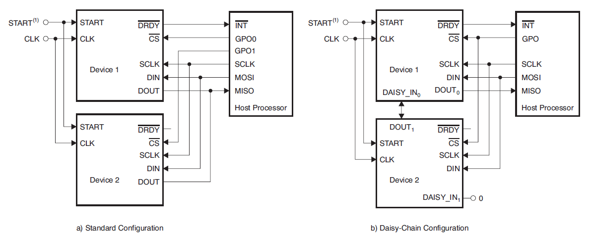
I am planning to use both ways together daisy chain and cascaded mode 。I want to be able to configure each ADS separatelly, so I need cascaded mode, then receive data in daisy chain mode.

I have some questions in the following:

1.   Eight ADS1299 in Daisy-Chain mode,data rate = 1000 SPS.Reading the register data every millisecond. Do I treat the values of these 8 registers as the one register and read them out, or do I read the data of the 8 ADS registers in turn? An ADS has 27-bit registers,So do I read the data of the 216-bit register every 1ms?

2.  If I use cascade mode to read data,do I need to switch 8 CS pins back and forth in 1ms?

Best Regards

  • Hi Peanuts,

    Thank you for your post and welcome to our forum!

    Reading register data is a different operation than reading ADC conversion data. You must exit the RDATAC mode before issuing a RREG command. After the RREG command is recognized, each ADS1299 device will load register data into its own output shift register. Register data cannot be overwritten with ADC conversion data, so there is no time limit to read the data.

    Each ADS1299 has 24 registers. To read all register contents from all devices in Daisy-Chain Mode:

    1. Bring all /CS pins low
    2. Send 0x20 0x17
    3. Send 192 bytes of 0x00

    To read all of the registers in Cascaded Mode, you will need 8 separate MISO (i.e. DOUT) connections to your host controller. The procedure is the same as for Daisy-Chain Mode, except fewer SCLKs are required:

    1. Bring all /CS pins low
    2. Send 0x20 0x17
    3. Send 24 bytes of 0x00

    Best regards,

  • Thank you very much Ryan ,Maybe my second question was misexpressed,sorry.

    I use cascade mode to read data,which refers to reading ADC conversion data, not the value of the register.

    1.To read all of the ADC conversion data in Cascaded Mode,1ksps,do I need to switch 8 CS pins back and forth in 1ms?

    2.To read all ADC conversion data from all devices in Daisy-Chain Mode.Are the following operations correct:

            1)Bring all /CS pins low

            2)Enter RDATAC mode

            3)Read 216 bytes of data(27*8)

    Best regards

  • Hi Peanuts,

    1. In Cascaded Mode, all conversion data must be read within 1 ms. You will assert /CS1, read 27 bytes from Device 1, deassert /CS1, assert /CS2, read 27 bytes from Device 2, etc. Note that you will have to account for small timing delay requirements between /CS and SCLK edges for each device.
    2. You are correct.

    Best regards,

  • Thank you very much Ryan

  • hello

    Ryan Andrews, Alexander Smith,

    I now want to collect data simultaneously by using 4 pieces of ADS1299. In Daisy chain mode, I want to know all the register data of ADS1299.

    My understanding is that CS is set low, all ADS1299 are selected, and then 0x20 and 0x17 instructions are sent. Each ADS1299 receives the same register instruction, and then the register data of each ADS1299 will be sent to the first PIECE of ADS1299 through DAISY_IN0, and then returned to the STM32 chip.

    Here's what I did

    1, I'm going to lower all the CS

    2, send 0x20, 0x17

    3. Read 96 register data at one time through SPI

    But I may have reached the register value of the first slice of ADS1299, and the other ADS12999 values are 0x00.

    Is there anything wrong with this interpretation?

  • Hello,

    Are you saying that you have tried this and your results show all 0x00 after Device 0 registers are read?

    Remember that:

    • DOUT3 -> DAISY_IN2
    • DOUT2 -> DAISY_IN1
    • DOUT1 -> DAISY_IN0
    • DOUT0 -> MCU MISO

    All /CSn pins must remain low throughout the entire sequence and all devices must receive the same DIN and SCLK signals.

    Regards,