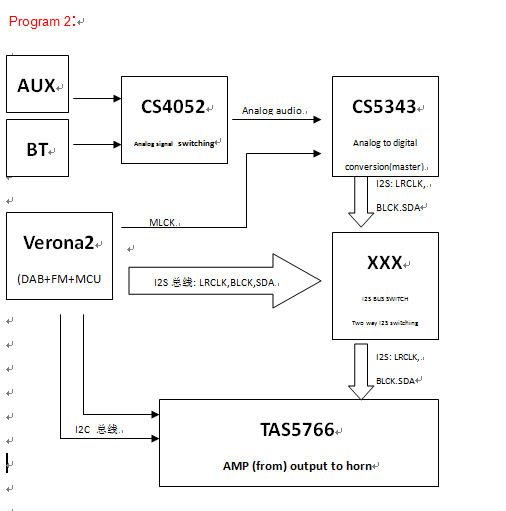
For the design of the TAS5766, according to customer requirements, such as accessories to describe two sets of programs, please help confirm the feasibility of the two program
1 Program 1 / two for the TAS5766 is largely omitted from the I2S MCLK master clock line, is it feasible? What impact does it have on TAS5766?
2 in the first scheme, the I2S bus switch in the DATA line, whether it will affect the timing of the I2S? TAS5766?
3 in the first scheme, the I2S bus in the DATA line, after a switch (such as 74HC151), the other line does not pass, will affect the timing of the I2S?
4 in the second scheme, the overall switch I2S bus, if my I2S sampling frequency is different, TAS5766 can brake identification?
5 in the second scheme, the overall switch I2S bus, if my I2S sampling frequency is the same, the impact on the TAS5766?
6. How to update I-RAM Block, C-RAM Buffer A / B data when playing? Can you provide an example?