This thread has been locked.

If you have a related question, please click the "Ask a related question" button in the top right corner. The newly created question will be automatically linked to this question.

PCM1795: PCM1795

Part Number: PCM1795
Other Parts Discussed in Thread: TINA-TI,

The question relates the parameter "Center current At BPZ -3.5 mA".

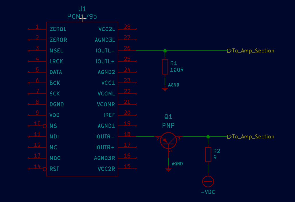
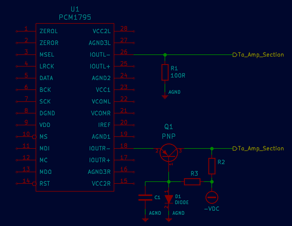
I do not use op amps, I sense the output current via a low value resistor, or a transitor in a common base configuration.

In the case of sense resistor, I measure -3.36 mA, invariably.

In the case of transistor, I measure -4.66mA.

How it is possible? I've read the datasheet several times in search of something that could explain this behavior, but I can't understand it.

Thank you in advance for your answer.

  • Hi Angelo,

    Do you think you could share a schematic? I do not quite understand your output configuration.

    Thanks!
    Paul
  • Hi Paul.

    This is a sample circuit, just to explain you my question.

    The case of R1 at the output pin 26: I have to read 350mV at "To_Amp_Stage" point with respect to AGND. I read, instead, 336mV.

    The case of R2, Q1 at the output pin 18: the current flowing through resistor R2 must equal, if we neglect the Ib, the current of 3.5mA, as stated in the datasheet. I read 4.66mA.

    Take into account that the latter circuit is a simplified version of the real one: the base of transistor Q1 is tied at a voltage that bring the emitter at AGND potential.

    Why this behavior?

    Thank you

    Angelo Adamo

  • Hi Angelo,

    I am not sure why you are seeing this behavior, as your simplified circuit looks okay. You could verify the voltage on DAC output pin (pin 18). Note that most ICs have ESD diodes on their pins, so if the pin is forced below 0V, it could be sourcing current from GND. You could also share your actual circuit and we could take a look at that as well. Otherwise I would also do a thorough visual inspection to ensure there is no flux or solder issues.

    Thanks!
    Paul
  • Hi Paul.

    Thank you for your answer.

    This ia a more realistic drawing of my circuit:

    It represents an I/V converter that doesn't use an operational amplifier; simple, linear, no feedback at all.

    The drop on D1 compensates the b-e voltage drop: the voltage I read at pin 18 is +48mV. The same happens at pin 26 which uses the same circuitry and were the voltage is +49mV.

    I have several items like this, all showing the same issue.

    Angelo

  • What are the values of R2, R3, and -VDC?
  • The VDC = -5V, R3 = 47K, R2 = 374R. There is also a resistor of 768R from collector of Q1 to AGND; its purpose is to stabilize the collector voltage at 1/2 VDC. If you calculate the currents and voltages regulating the circuit, you will find that voltage at the collector must be equal to -2.5V, while I read -2.19V. This lead to desume that the resulting current flowing out of the output is 4.66mA, not 3.5mA.
    All the above reveals the whole philosophy of the circuit. If you want, I can also give you the equations that regulate its operation.

    Thank you.
    Angelo
  • Hi Angelo,

    I am having trouble visualizing your output stage.  Wouldn't there be additional current flowing between the 768Ω and 374Ω resistor and -5V? 


    I have attached a TINA-TI circuit as well.PCM Output IV.TSC

  • Hi Paul.

    I apologize, the schematic is incorrect, the diode should be reversed: anode must be connected to AGND, not cathode.

    Anyway, I attached the correct TINA-TI file, where, instead of a diode, an additional pnp transistor of the same type of Q1 is added.

    If you do the DC analysys and the current issued by the current generator is 3.5mA, voltage at VF2 point results -2.49V and everything works properly.

    If you set the current at 4.66mA, then the voltage at VF2 point becomes -2.2V. You may verify that also doing simple current/votage calculations. This is the situation a have on my circuit, and I'm trying, with your help, to understand why.

    Angelo

    This is the file: https://drive.google.com/file/d/1_Cs5tYWwxzFAyA9eBYy7C3vkctuO0lJh/view?usp=sharing 

  • Okay,

    First I would confirm that the device is powered on correctly, and then I think the best next step would be to measure the actual current from the output. I have not seen any issue with the PCM1795 where it would source additional current, but maybe if the part is biased incorrectly then there could be some current flowing from the ESD diodes on the output.

    Thanks!
    Paul
  • Hi Paul.

    The component is powered correctly, so much so that it works regularly and the sound quality is excellent.
    I measured the current by means of a digital voltmeter; I used it as a 20mA scale ammeter and connected it directly between an output and AGND. The current I measured is 3.36mA, not 3.5mA.
    The output in question was floating and I could perform the measurement.

    How can I measure the current with an instrument if a circuit like the one described is connected to the output? I can only describe it, as I think I demonstrated with the simulation that I attached to the previous email.

    Be sure, the circuit is polarized correctly. There are dozens of devices that work perfectly, but with the uncertainty of the 0dB output current.

    On the other hand, if the additional current were due to the ESD protection diodes, its value would vary greatly between one output and another, between one device and another. Instead, the circuits behave exactly all the same way.

    The only way, I think, to take a step forward is to make the circuit as a scheme, if it is not too demanding for you. The circuit is completely described and all (few) components have a value.

    Angelo

  • Hi Paul.

    Do you have any news for me?

    Best Regards

    Angelo

  • Hi Angelo,

    I think it is unlikely that I will be able to build to your exact circuit, but a good test would be to confirm the IOUT current by inserting an accurate meter between the output pin and Q1. Then, with meter still connected, short the Q1 side of the meter to ground. If the current changes, then we can be pretty confident that there is some circuit issue with the output stage.
  • Hi Paul.

    I'm sorry, but what you ask is almost impossible. The transistors are packaged in a TSSOP6: their body measure 1.2mm x 2.2mm, the pich among pins is 0.65mm. Lifting a pin of it from the printed circuit board is impossible for me without risking to break everything. From the pcm1795 side is the same: pin pitch is 0.65mm.

    Anyway, I gave you the information about the real output current measuring its value with an ammeter set to 20mA full scale and connecting it between the pin and AGND: the value I measured is 3.35mA, not 3.5mA.

  • Hi Angelo,

    Any new developments on your end? Do you think you could share your schematic for the PCM section? Do you have anything besides a cap connected to the VCOM pins?
  • Hi Angelo,

    I would like to point out that the bias current can be impacted by the IREF , VCOML, and VCOMR pins. I think you should verify that you have the recommended resistor and caps on those pins. In addition, you could look for potential build issues on those pins - solder bridges, excess flux, dry/cold solder joints.

    Thanks,
    Paul
  • Hi Paul.

    This is the schematics of PCM1795 circuitry. The I/V circuits attached to IOUTxx pins are that I showed you in the previous messages. The TINA-TI model represent exactly the circuits I use.

    The capacitor C32 in the drawing is a couple of 22uF paralleled, so the total capacity is 44uF, not 22uF as reported.