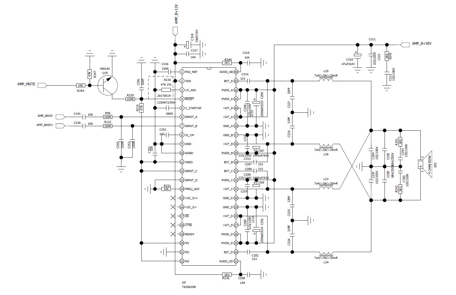
This thread has been locked.
If you have a related question, please click the "Ask a related question" button in the top right corner. The newly created question will be automatically linked to this question.
Dears :
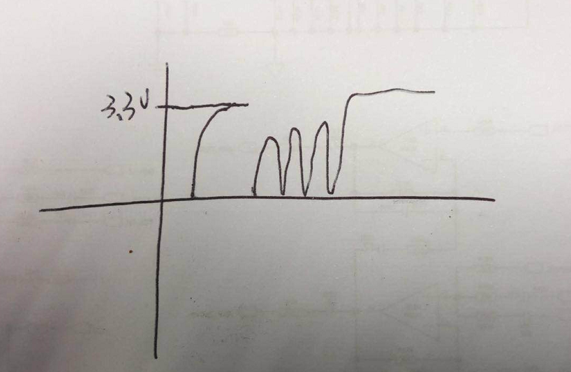
TAS5630B damaged in PP, total 100 PCS of 200, fail ratio is 50%. I found abnormal waveform on RESET PIN when switch Signal source , the voltage on RESET pin usually is 3.3V, but when did fast switch signal source ,the voltage will drop to 1V or 2V, attachment is the sketch for your REF. Could you please help check if this operation can cause TAS5630B damaged ? Thanks .
Hi Haiwen,
Have you checked the FAULT pin? Did the FAULI happen?
What about the inductor spec of the output?
Can you share the schematic to us?
Derek,
Regards
Yanming:
fault pin is floating , attachments are the schematic and indicator spec for your reference . PBTL mode is much easy burning , BTL mode is less burning . Could you please help check the root cause ?Thanks .
Hi Haiwen,
The unused Input pins can not be connected to GND directly. They should be connected GND by capacitors.
Derek,
Regards
Hi Haiwen,
Sorry, I made a mistake. The input design is fine.
I suggest to disconnect the reset pin to CPU. Remove the Q18, just pull up the reset pin to high, and try again.
When reset the device, there will high peak current on output, so we suggest high rate current inductor.
Please also pay attention to the device thermal.
Derek,
Regards