This thread has been locked.

If you have a related question, please click the "Ask a related question" button in the top right corner. The newly created question will be automatically linked to this question.

LMK04828: OSCin clarifications

Part Number: LMK04828

Hello Guys,

Good day.

According to our customer  single-ended AC coupled inputs in the LMK04828 evaluation module (SNAU145B-May 2013 - Revised march 2018) uses the negative input for OSCin_N and CLKin_N instead of the positive leg _P. Is the "inverted" input connection necessary or using the _P inputs for these single-ended signals also acceptable?

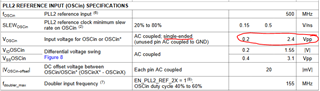
Also, just like to confirm if the OSCin inputs in AC coupled single ended config can be driven by a 3.3V signal?

Thanks and regards,

Art

  • Art,

    They can use the positive leg _P for either input. OSCin uses only _N input because the VCXO manufacturer frequently alternates between 6-pin footprints and 4-pin footprints in the same package, and OSCin_N is connected to the output pin that is always present. CLKin1_N choice was arbitrary.

    OSCin maximum single-ended AC-coupled signal swing is 2.4V. The OSCin buffer is slightly different design from the CLKin buffers. Signal swing in excess of these limits can compress the input stage and increase the close-in phase noise.

    If driving with a 3.3V source e.g. LVCMOS is required, it is recommended to use a resistor divider to reduce the signal swing. For instance, R4 and R61 on the EVM form a divider which attenuates the ~3V LVCMOS output of the VCXO to around 1V.

    Regards,

    Derek Payne

  • Thanks for looking into this Derek. 

    Customer have additional inquiries

    "If the CLKin or OSCin inputs are not resistor divided to lower the voltage and left at 3.3V, AC coupled single-ended, is there concern for damaging / overstressing the LMK's input or drawing excessive current? Or increased phase noise is the "only" concern? Can it be quantified how much worse the phase noise gets?"

    Thanks and regards,

    Art

  • Good day Derek.

    Just like to update on the follow-up inquiries from the customer.

    Best regards,

    Art

  • Art,

    Thanks for the reminder ping, for some reason I wasn't notified on this thread.

    There's a few effects that can happen, depending on the voltage excursion beyond recommended range and the slew rate of the signal:

    • From about 2.4V to 3.0V signal swing, this pushes the input amplifier structure into compression. This has no long-term effects on device operation and shouldn't cause any noticeable change in current consumption, but in compression the input stage BJTs are saturated and it takes slightly longer for them to recover back to linear operation. The exact effect this has on the phase noise is hard to quantify, and depends a lot on the waveshape and the slew rate; I would expect no more than a few dB of degradation overall, worst case. Anecdotally, I often run our sine wave signal generators at +14dBm into the LMK04828 CLKin stage with 10MHz waveforms, because the slew rate on a 10MHz sine wave is not normally high enough to achieve a consistent lock; I don't recall ever seeing the impact on PLL noise exceed the close-in noise of the reference. But I have seen elevated PLL noise by one or two dBwith a +14dBm 100MHz Wenzel oscillator into OSCin...
    • Above 3.0V signal swing, depending on slew rate, the input current across the internal AC-coupling to the BJT input stage can cause overshoot and undershoot tripping the clamp diodes on the input. There will not be much effect from a sine wave that just barely exceeds the acceptable margin, since the slew rate at the peak and trough of the sine wave is very low. But for example an LVCMOS 3.3V signal may see overshoot and undershoot that stresses the input clamp structure long-term, especially at hot temperatures.
    • An additional uncommon consideration: the internal common mode bias generator circuit on OSCin pins is nominal 1.7V, and there are three antiparallel diodes clamping the signal swing from P to N (hence the differential signal swing limitations). But that common mode is only nominal 1.7V, and can shift across process and supply voltage by ±100mV... if the single-ended signal swing is too large and the common mode is offset from the nominal value, these antiparallel diodes can be activated and the unused pin voltage can be pulled up or down. Since the recommended circuit for the unused pin is a 0.1µF capacitor to GND, at very high signal swing this can cause high power dissipation within the clamp structure, and eventually this clamp structure may degrade or fail, greatly impacting the phase noise or even damaging the OSCin buffer beyond use.

    The limits in the datasheet are specified for a reason, and the customer should try to follow them.

    Regards,

    Derek Payne