This thread has been locked.

If you have a related question, please click the "Ask a related question" button in the top right corner. The newly created question will be automatically linked to this question.

LMK05318B: Some questions about LMK05318B

Part Number: LMK05318B
Other Parts Discussed in Thread: LMK5B33216

Hello Expert,

Our customer is considering to design this part.

So there are some questions as below.

I want to get your feedback about each items.

1. If there is EVM or Design file (Schematic, PCB) or Design guide, please let me know.

    I couldn't find them.

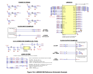
2. Is it possible to set OUT0/1, OUT2/3 to OUT0, OUT1, OUT2, OUT3 with different frequency outputs? Or is it the same frequency output?

    Is it possible to output with separate frequencies? Are they tied together?

    When I check register and block diagram, it seems to tied OUT0/1, OUT2/3 together.

3. When using two products for 16port output, is output clock skew control possible?

    They want to remove clock skew on output.

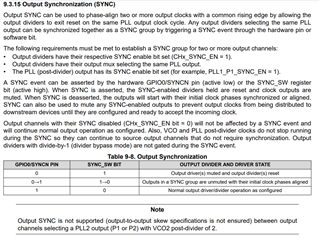
4. About Ref. Clock:

    Can I use only either DPLL or APPL? or Should I use all of them?

    They think that reference clock is burden.

    When I check block diagram, I think that both reference clock input is needed.

5. What's minimum output frequency of AC-LVDS?

    There is no commented on the data sheet.

    Our customer need min. 100khz.

Best regards,

Michael

  • Hello Michael,

    1. Yes, we have an EVM user guide. Here is the link: LMK05318B EVM User Guide

    The EVM user guide has our EVMs schematic and layout that can be reference for your systems design.

    Figure 10-4 in the data sheet also shows the LMK05318B reference schematic design.

    I have also attached a how to build a LMK05318B schematic guide below as well.

    How to Build a Schematic for the LMK05318B.pdf

    2. OUT0 and OUT1 must output the same frequency. OUT2 and OUT3 must output the same frequency. OUT0 and OUT1 share a channel divider, so it is not possible to output different frequencies. The same applies for OUT2 and OUT3.

    3. The LMK05318B has an output synchronization feature that can be used to synchronize the phase of the output clocks. Section 9.3.15 in the data sheet provides an explanation of the output synchronization feature.

    In regards to aligning the phase of two devices, you would need to:

    a. First use the output synchronization feature to synchronize the output clocks of the first device.

    b. Then feed one of the outputs of the first device to the input of the second device and use the zero delay mode (ZDM) feature of the second device to synchronize the input clock with OUT7 of the second device.

    c. Then use the output synchronization feature of the second device to synchronize the phase of the second devices output clocks with OUT7 (thereby synchronizing the outputs of the second device with the input of the second device and thereby synchronizing the output clocks of the second device with the outputs of the first device).

    If 16 outputs are required, I would recommend using our LMK5B33216. This device is the 16 output version of the LMK05318B with some additional features such as a 3rd APLL and APLL DCO (for frequency and phase adjustments performed directly to the APLL).

    4. The APLL must always be used for the device to operate, but the DPLL is optional. Here is a document that provides a description of how the LMK05318B operates. This document should clear your understanding of how the APLL and DPLLs are used. I strongly recommend reading through this entire document.

    How the LMK05318B Operates.pdf

    5. OUT0 to OUT6 can output an AC-LVDS clock from 3.0692 MHz to 800 MHz. OUT7 can output an AC-LVDS clock from 1 Hz to 800 MHz.

    The LMK5B33216 can allow for up to 12 outputs to generate clocks from 1 Hz to 1250 MHz.

    Please note the LMK5B33216 has the output synchronization feature as well, so you can phase align all of your output clocks.

    Regards,

    Kia Rahbar

  • Hi Kia,

    Thank you very much for reviewing the schematic in the past.

    I have an another question as below.

    Our customer will use oscillator for reference clock input.

    When I compared reference circuit of data sheet and EVM, there is some differences.

    Could you please let me know which circuit should I use?

    1. Application circuit of data sheet

    2. Application circuit of EVM

    Best regards

    Michael

  • Hello Michael,

    For a single-ended XO input, the recommended termination is as follows:

    In the data sheet image, the capacitors are placed for an AC-coupled LVCMOS input, and the 100 ohm and 50 ohm resistors are used as a voltage divider to step down the swing of the OSC from 3.3 V to 1.1 V.

    In the EVM image, the 33 ohm is to match the 17 ohm output impedance of the OSC and the 220 ohm and 240 ohm are used as a voltage divider to step down the swing of the OSC from 3.3 V to 1.7 V.

    I would recommend using the termination shown in the image I have just shown at the beginning of this message.

    Regards,

    Kia Rahbar