Other Parts Discussed in Thread: LMK1D1204
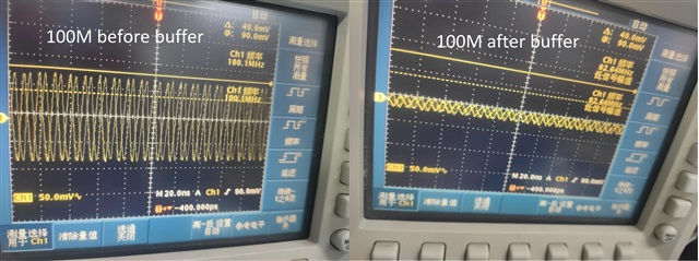
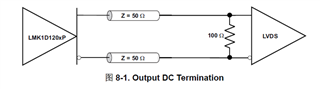
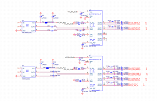
Problem 1: LMK1D1208P is used as the clock buffer. Three 100Ms from the same chip are used as the system clock of three FPGAs. Two of them are OK. One of them has a problem with the clock when debugging DDR3. After replacing the system clock, there will be no problem. The DC coupling method is used:
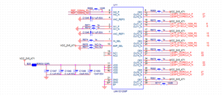
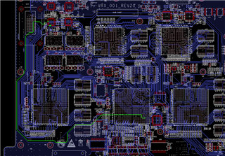
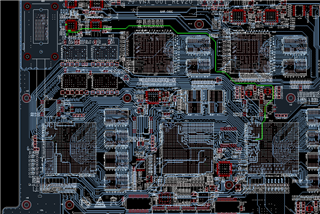
The following is the PCB routing of two DDR3 without problems:
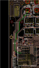
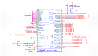
The following is the clock routing of a faulty FPGA:
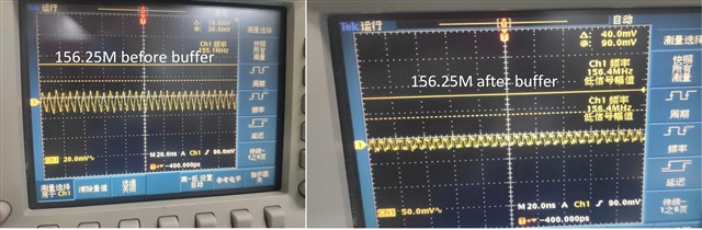
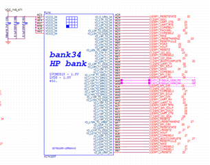
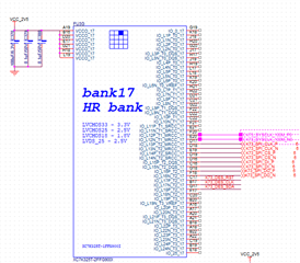
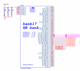
Problem 2: Two LMK1D1204 chips, 156.25M and 100M, are used to provide clocks for the high-speed ports BANK116 and BANK115 of the FPGA. The 156.25M BANK116 clock is not locked, and the 100M BANK115 is used to lock. When the 100M BANK116 is used, it is also locked,:
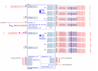
The length of 100M PCB wiring is 3712.15mil, and the length of 156.25M PCB wiring is 4357.63mil. The PCB wiring diagram is as follows: