


Hi team,
My customer is considering using multiple CDCE925s on a board, and has question on its slave address setting.
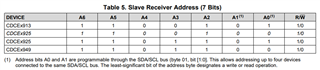
On the datasheet, Table 5 shows slave receiver address. It states that A1 and A0 are programmable, and user can address up to four devices connected to the same SDA/SCL bus. Table 9 shows register configuration, and it looks like OFFSET [01h] BIT [1:0] is for setting slave address.
Does TI write this address for the customer before shipping, or should the customer write it after getting CDCE925? If it is latter case, then when multiple CDCE925s are on the same I2C bus, all CDCE925s will have same address setting. So the customer needs to write before implementing CDCE925 on PCB, am I correct?
Best regards,
Kurumi