- Ask a related questionWhat is a related question?A related question is a question created from another question. When the related question is created, it will be automatically linked to the original question.
Hi team,
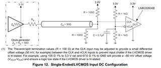
In TI's 4xAWR2243 cascaded imaging radar reference design TIDEP-01012 reference design | TI.com, the LMK00804B's nCLK input is DC-biased to 0.7V with resistor ladders as below:
the 40M_BUF_ IN_ PRIMAWRY clock is from AWR_1_OSC_CLKOUT, which is a gound to 1.4V swinging square wave.
And I was little confued about the input DC-bias, WHY the Non-inverting differential clock input is not DC biased to 0.7V? Isn't it supposed to both differential clock inputs are DC-biased?