Part Number: CDCV304
Hi
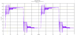
We are using two CDCV304 clock buffer in same control card and we are getting different waveforms from these 2 buffer outputs.
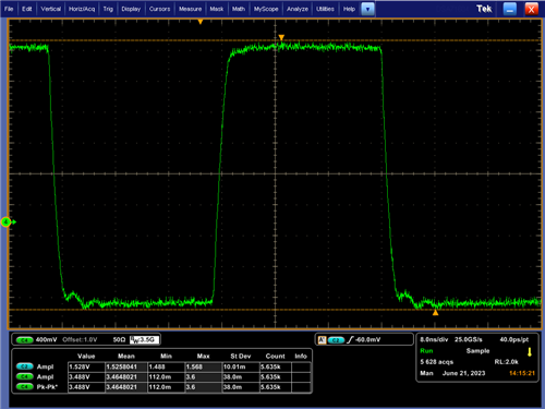
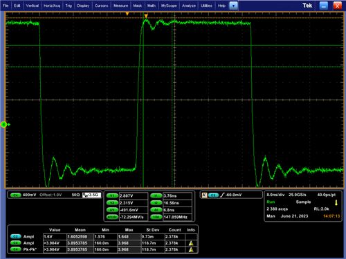
These 2 buffer output is going to same receiver with 33 ohms termination. For 1 buffer clock output there were no ringing & as for other output ringing is there. Attached the waveform below.
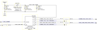
|
S.No |
Net name |
CLK Freq |
Driver |
Receiver |
Series R |
TL length from Driver to Rx |
Captured Waveform |
|
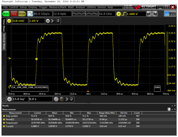
1 |
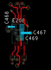
CLK_10M_20M_1588_OCXO |
20M |
CDCV1 |
Xilinx Kintex 7 FPGA |
33 ohms |
16.2 inch |
 |
|
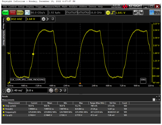
2 |
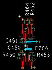
CLK_125M_APLL_1588_FBCK |
125M |
CDCV2 |
Xilinx Kintex 7 FPGA |
33 ohms |
3.8 inch |
 |
|
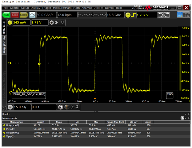
3 |
20MHZ_PLL_OSC_CLK |
20M |
CDCV1 |
RC 8A35036 SMU |
33 ohms |
9.6 inch |
 |
|
4 |
CLK_125M_PLL_1588_FBCK |
125M |
CDCV2 |
RC 8A35036 SMU |
33 ohms |
4 inch |
 |
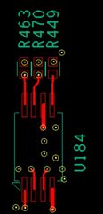
By varying the termination resistor value to 22 ohm, 18 ohm, 10 ohm still we are seeing ringing with overshoot & undershoot in the waveform.
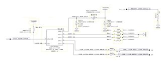
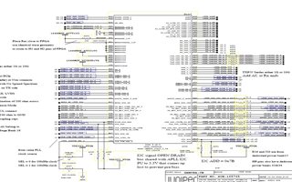
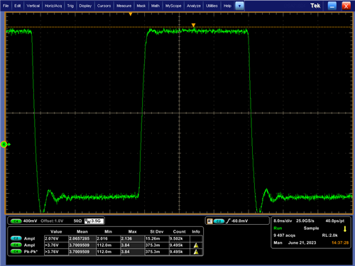
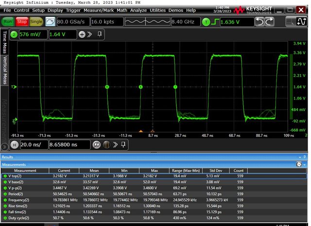
I have checked the input clock for CDCV304 (CDCV1) and it is fine, attached the same here for your reference.
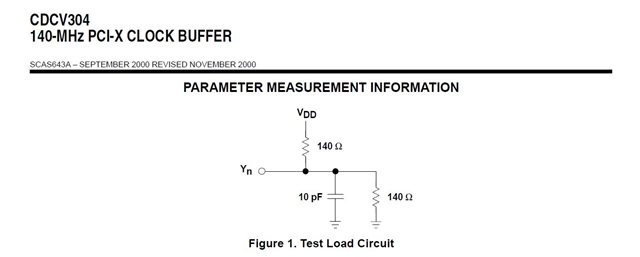
Load circuit test given in the datasheet is for 70 ohms instead of standard transmission line impedance of 50 ohms.
Our PCB traces are routed using 50 ohm impedance. Do you think this could have caused the issue?
Kindly help us understand the reason for the ringing.
Thanks
Mohan