This thread has been locked.

If you have a related question, please click the "Ask a related question" button in the top right corner. The newly created question will be automatically linked to this question.

CDCE913-Q1:Operation of the Y2 output pin at power-on

Part Number: CDCE913-Q1
Other Parts Discussed in Thread: CDCE913

【question】

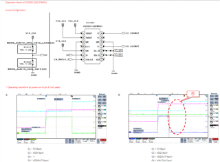
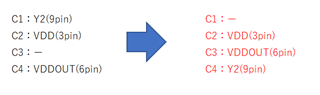
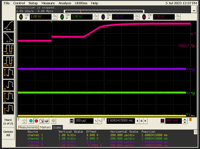
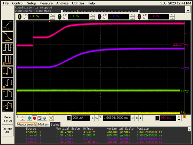
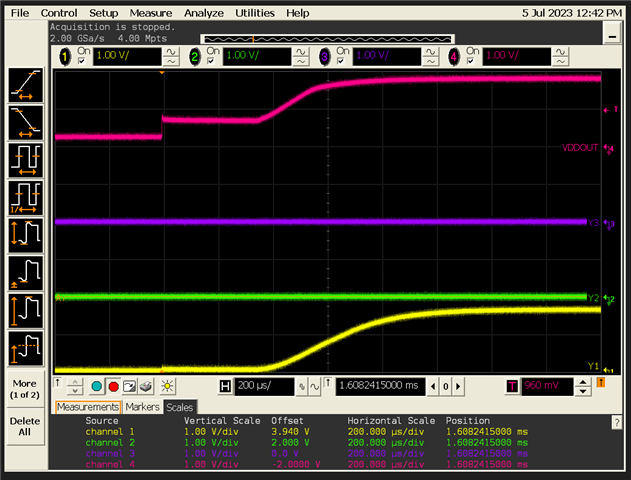
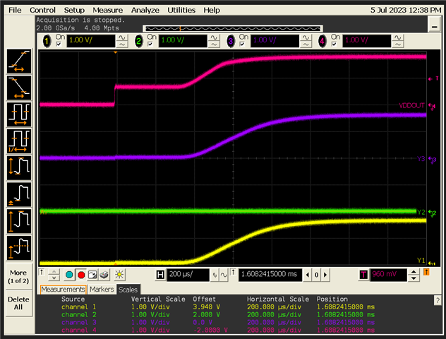
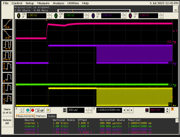
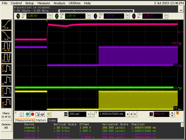
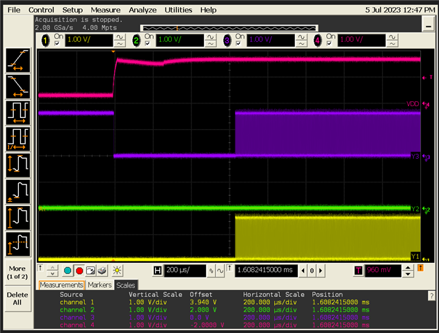
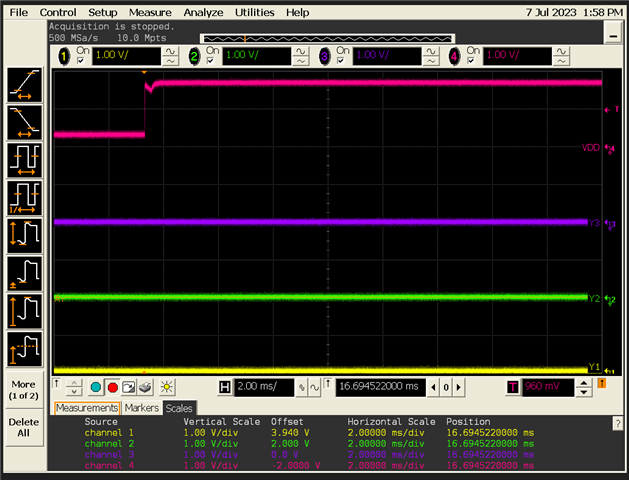
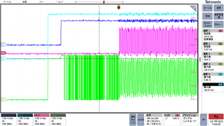
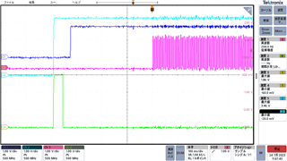
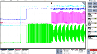
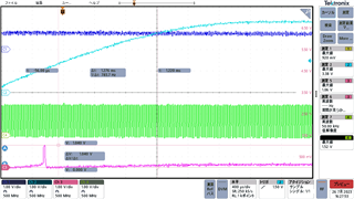
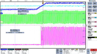
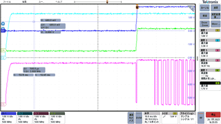
・Regarding part Ⓐ indicated by the dashed red circle, the waveform of board 1 in ① and the waveform of board 2 in ② have different timings when Y2 (9pin) falls from H to L. Why? mosquito?

・I can understand the movement of Y2 (9pin) from H to L in the waveform of board 1 in (1) (changes to L when VDD (3pin) turns ON), but in the waveform of board 2 in (2) It is unclear why the timing of Y2 (9pin) changing from H to L is this timing. Please tell me why this is the timing.

  • Satoru-san,

    Do you have a capture where Y2 is present for the left case? In the left capture, the caption states that Y2 is on Channel 1 of the oscilloscope, but only channels 2, 3, and 4 are being shown.

    Or are the labels provided for the captures different than what they actually represent?

    Thanks,

    Kadeem

  • excuse me. I made a mistake.
    The waveform on the left has the following channel configuration (red).

    Thank you.

  • Satoru-san,

    I do not believe that we have a timing specification for this configuration. It may not be the same from part to part.

    If the sequencing of the supplies is reversed (VDD before VDDOUT), is this behavior still observed?

    If the two parts are swapped, is the behavior the same for each part, or is it board-specific?
    Thanks,

    Kadeem

  • I was told that the power sequence in which VDD and VDDOUT are opposite (VDD rises first) is not good for the device, so I am not thinking about changing the current power sequence.

    In the left and right waveforms, the timing at which Y2 (pin 9: unused and set to Hiz) changes from H to L is different, and the left side seems to change to L in sync with VDD, but the right side. I would like to know if you know at what timing it changes to L without synchronizing with VDD.

  • Satoru-san,

    I will check with our design team and see if this information is something that we have characterized.

    If we do not, I will investigate this behavior on the bench.

    Thanks,

    Kadeem

  • How is the confirmation status with the design team? Did you understand anything?

  • Satoru-san,

    I have reached out to the design team on this a couple of times with no response.

    I have a couple of samples shipping to me this week so that I can evaluate this across a few parts to check the behavior with this configuration.

     Thanks,

    Kadeem

  • Kadeem Samuel
    Have you received any response from the design team?
    Also, could you conduct an evaluation?
    Please let me know the result.

  • Satoru-san,

    Sorry for the delay, we have been on holiday for the past two days. I have received the samples with this configuration.

    I will have to perform a bench evaluation for this case over a couple of parts - expect a response by 7/7 once I have checked over multiple parts to confirm if this behavior is expected and repeatable.

    Thanks,

    Kadeem

  • Satoru-san,

    On the first part, I see VDDOUT rise with no output clocks rising about 80% of the time:

    About 15% of the time either Y1 or Y3 rises after VDDOUT is applied. These clocks stay high for about 650us after VDD is applied, after which they output at the correct frequencies.

    About 5% of the time, both Y1 and Y3 rise after VDDOUT is applied. These clocks stay high for about 650us after VDD is applied, after which they output at the correct frequencies.

    Additionally, whatever state the clocks are in initially gets toggled when VDD rises - see below:

    During no part in this process does Y2 go high. I will relay my findings here to the design team as well.

    Thanks,

    Kadeem

  • Kadeem Samuel
    Thank you for your evaluation.

    Below is what I would like to confirm.
    It is still easy to understand why Y2 is pulled by VDDOUT and becomes Hi.
    The waveform on the left side of the waveform I sent is that when VDD goes Hi, Y2 goes down to GND, because the device's internal control logic starts to operate, so I think there is no problem if it operates like that. However, in the waveform on the right, Y2 drops to GND before VDD goes high. This is why Y2 changes from Hi to Low (GND) before VDD is applied (before the control logic starts operating). I want to know why.

    Thank you very much.

  • Satoru-san,

    This is what we are still trying to determine the root cause of, which is more difficult when we are not able to replicate this behavior on the bench.

    Are you seeing this as consistently repeatable on your end where Y2 changes state before VDD is provided across multiple power cycles and multiple devices?

    Thanks,

    Kadeem

  • Mr. Kadeem Samuel
    Thank you for contacting us.
    We will check it multiple times with our board.
    We only have two of our boards available, but we will try to check each of them multiple times. We will contact you again when we have confirmation.

    Also, I have an additional question. In the waveform you sent us, it is stated that the oscillation occurs at a normal frequency after 650μs, but when the oscillation starts, is the frequency as set from the beginning?
    On our side, it seems to take about 10ms from the time VDD rises until the clock starts outputting. (for both Y1 and Y3).
    Are there any possible causes?
    Does the circuit to which it is connected have any effect?

  • Mr. Kadeem Samuel
    I am very sorry.
    The above question that you asked today, that it takes about 10 ms for the output frequency to be output, has been resolved, so please disregard it.

    On another matter, when the input clock (CMOS clock) is not input, is it correct to assume that the output clock is indefinite?

  • Satoru-san,

    Just checking to ensure that I understand your question - if there is no input clock, is there any output, glitch or otherwise, on the clock outputs?

    I checked this condition a few (20) times - in each case saw a result similar to below:

    When there is no input clock, the PLL is unlocked, and the outputs are low.

    Thanks,

    Kadeem

  • Dear Khadeem Samuel.
    Attached below are the waveforms at power on.

    C1: Y1(18.432MHz)
    C2: VDD(1.8V)
    C3: VDDOUT(3.3V)
    C4: CLKIN(19.2MHz LV-CMOS)

    C1: (18.432MHz) outputs an undefined frequency, not the set clock frequency, until C4 (19.2MHz) is input.
    Although there is no waveform, the 12.288MHz output of Y3 also behaves in the same way.
    Y2 goes High when VDDOUT rises, then goes Low and stays Low.
    (The waveforms are also attached.) Each channel is the same as above, only C1 is changed to Y2.

  • Hello Satoru-san,

    Kadeem will be on vacation for the next few week so I will be answering in his place.

    Please provide an update to this question: "Are you seeing this as consistently repeatable on your end where Y2 changes state before VDD is provided across multiple power cycles and multiple devices?" We need to know if the error is reproducible.

    I will try to replicate the results again as well as follow up with the design team regarding this issue.


    Thanks,

    Kyle

  • Mr. Kyle Yamabe
    Thank you for your help.

    It is the output state of Y2, but it is not always the same every time,
    Sometimes it is on the left side of the first waveform I sent you, sometimes it is on the right side, and so on.

    Also, I am concerned about one more point. As shown in the waveform I sent you the other day, Y1 and Y3 output the clock before the input clock is input (not at the set frequency).

  • Hello, Majima-san

    The behavior of Y1 and Y3 producing random frequencies is most likely due to the noise while the clock input (C4) is LOW. The noise is being detected by the PLL which tries to create a frequency. I would recommend turning on the input clock (C4) before VDO and VDDO. This ensures that while the device is on, there will always be the correct input clock. I have also confirmed with the designers that XIN/CLK is failsafe so no issue should occur while the Clock input is HIGH but VDD and VDDO are LOW. 

    For the HIGH portion of Y2 this may be occurring due to coupling between the input to the clock generator and other parts of your circuit, which makes it difficult for us to replicate this result in our lab. For this reason I suggest solving this issue by supplying the device with VDD before VDDO. This will force Y2 to stay LOW  since it will be controlled and limited by VDD. Stated in our data sheet on the part we do not have a power-up sequence restriction, so please try powering up the inputs in this order 1. Clock input(C4), 2. VDD(C2), 3. VDDO.(C3)

    Thank you and please let me know if you have any other issues

  • Hello, Mr. Yamabe.
    Regarding the power supply sequence, in the QA list exchange with your company, it was answered that VDD(1.8V) must be kept at GND level until VDDOUT(3.3V) reaches a certain voltage, otherwise a large current may flow to the VDDOUT pin. Therefore, for our products, power is applied in the order of VDDOUT(3.3V) Arrow rightVDD(1.8V).
    This cannot be changed now.
    Also, I was told that if CLKIN is also at GND level, the clock is not output until the PLL is locked (GND level),
    I have configured the circuit so that CLKIN is also clocked in after the VDDOUT/VDD power supplies are turned on, and this cannot be changed now.

    *This answer is inconsistent with the answers I have received so far in the QA with your company, does this mean that the answers in the QA list were wrong?

  • Hello, Majima-san

    Can you please direct me or add me to the QA list exchange. I would like to confirm if the information previously provided is correct.

  • Mr. Yamanobe.
    We would appreciate it if you could provide us with your e-mail address so that we can forward the QA list e-mail we previously exchanged.

  • Hello Majima-san,

    Please email me at k-yamabe@ti.com.

    Thank you so much

  • Hello Majima-san,

    For the power up sequence in the datasheet IF VDDOUT is applied first then it is best if you keep VDD at GND but you can also just apply VDD first and then apply VDDOUT. Both orders will work for the device. Are you able to test the device supplying VDD first then VDDOUT in order for us to confirm the problems?

    Can you tell me what is producing the CLIKIN? I need to confirm whether the CLKIN is floating or grounded while the CLIKIN is not powered. This may be what is causing the output problem.

    Also I am wondering why the CLKIN cannot be turned on before both power supplies? This E2E post discusses the power supply configuration and recommends to have CLKIN before VDDO and VDD. https://e2e.ti.com/support/clock-timing-group/clock-timing-internal/f/clock-timing---internal-forum/117389/cdce9xx-power-up-sequence?tisearch=e2e-sitesearch&keymatch=cdce9xx# 

    Thank you,

    Kyle

  • Mr. Yamabe,
    Thank you very much for your help.
    The sequence of each power supply of the first VDD and VDDOUT cannot be changed at present. Also, it is difficult to evaluate after changing it.

    As for the second one, CLKIN, I will send you the measured waveforms when a 10kΩ PD resistor is attached to the CLKIN pin (pin 1).
    There is no particular waveform difference between the case with PD and the case before without PD, and each output of Y1 and Y3 appears to output an undefined clock frequency until CLKIN is input.


    *Also, on this board, Y2 always changes from H to L before VDD is turned on. (10 times out of 10 power supply startups)

    The ch configuration of the measurement is described below.
    C1: VDD
    C2: VDDOUT
    C3: CLKIN
    C4: Y1 (first), Y2 (second), Y3 (third)

  • Hello Majima-san,

    Thank you for the pictures showing the outputs of the device.  It seems that the CLKIN is grounded since there was no difference with the Pulldown resistor.

    Are you able to start the clock input before VDD and VDDO to test the outputs? This would help me further confirm the issue with the device. Inputting CLKIN before VDD and VDDO will not cause problems to the device. The CDCE913 has internal fail safe circuitry to prevent any current damage.

    Thank you,

    Kyle

  • Mr. Yamabe,
    Thank you very much for your help.
    When I input the input CLK before VDD and VDDOUT are turned on, I found that about 0.7V is flowing into the VDD power supply pin.
    This state is not acceptable for our product because the VDD power supply (1.8V) is also used for other devices.
    Therefore, we cannot input CLK before turning on the power supply.
    We will send you the waveform at that time.


    The waveforms of VDDOUT and VDD not turned on (0.7V is flowing into the VDD power supply pin...) were checked, and it was found that CLK was not output to Y1.
    The waveform at that time is also sent.

    Also, with VDD and VDDOUT power turned on and no CLKIN, when VDD is turned on, CLKIN goes to Hi level and then an indefinite frequency is output.
    The waveform at that time is also sent.


    The measurement channels are shown below.
    C1: VDD
    C2: VDDOUT
    C3: Y1
    C4: CLKIN(1pin)

  • Mr. Yamabe,
    Thank you very much for your help.
    In addition to what I just sent you, I checked the state of the Y2 (unused port) pin when CLKIN is turned on before the VDD,VDDOUT power supply, and it was in a Low state all the time.
    We will send you the waveforms at that time.


    The measurement channels are listed below.
    C1: VDD
    C2: VDDOUT
    C3: Y2
    C4: CLKIN (Pin 1)

  • Majima-san,

    Thank you for all of the measurements and waveform. 

    From my understanding would the latest trials of inputting CLKIN first work for your design if the VDD pin on the CDCE913 did not reach 0.7V? 

  • Mr. Yamanobe.
    Thank you very much for your help.
    I am aware that when CLKIN is first input, it works as expected, except for about 0.7V flowing into VDD.
    However, the flow into VDD is unacceptable for the product as a whole. Also, due to the overall product design, it is impossible to input CLKIN earlier than the power supply of VDD and VDDOUT, and it will be the last. (Because CLKIN is supplied from the power supply IC: PMIC)

    Is it possible to avoid outputting CLK with an undefined frequency to the output clock when CLKIN is GND with VDD and VDDOUT power input to the IC?

  • Majima-san,

    Our team discussed adding Schottky diode on the VDD pin of the CDCE913 so even when it rises to 0.7 V on VDD it does not allow current flow to other systems. But from what I understand that is not an option either.

    To avoid the outputting CLK with an undefined frequency, since the other control pin configurations are set to have all outputs off - if a different control pin setting is used at startup (say, S2=1, S1 and S0 don't matter), are the outputs all off? Is there GPIO available for then changing the S0/S1/S2 states?