This thread has been locked.

If you have a related question, please click the "Ask a related question" button in the top right corner. The newly created question will be automatically linked to this question.

LMK04616: Holding outputs in SYNC using SYNC pin

Part Number: LMK04616
Other Parts Discussed in Thread: LMK04828, LMK04906

I have an application where I need to halt one of two clocks for a while (during a complex IO reset process) and then bring the clock back synchronously with the other clock (which must not be halted), maybe something like the figure below:

Is this possible?

As far as I can tell I can only stop selected clocks for any extended period of time using the SPI interface, which of course doesn't give me any control over the timing of the restarted clock.

  • You can choose which dividers participate in the SYNC process with the SYNC_EN_CHx bits. So you could assert an external SYNC signal on the SYNC pin and disable only the desired dividers. The divider reset generated by the SYNC pin is re-timed to the post-divider output of the VCO (or the clock distribution signal in distribution mode). So you could time the SYNC signal such that it arrives synchronously, and depending on when you release it, you could also restore the outputs at the same phase relationship with the other clocks before synchronization. This is the closest you can get to a "synchronous enable" function on LMK04616 - it's a bit convoluted, but it would work.

  • Thanks for the reply.  I was getting confused about the functionality of the SYNC input, in particular it turns out that I need to set SYNC_EN_ML_INSTAGE to 0 to enable level controlled SYNC.  With the default POR settings I was under the impression that only edge triggered SYNC operation was possible!

    Regarding edge alignment, I guess I'll have to see now it goes.

    I do have to say that the documentation is pretty horrible, it leads me in circles, and doesn't actually document key things.  I mean, in particular, what is the documentation for this key setting?  Here it is (section 9.6.2.212 [4]):

    SYNC Input Stage Enable Multi-level. When
    SYNC_INPUT_ENML is 1 the input stage is configured for
    multi-level mode.

    Oh.  "Multi-level mode".  Hmm.  What is that, I wonder?  This identical language occurs 7 times, for SPI_SDIO, SPI_SCL, SPI_SCS, STATUS0, STATUS1, CLKINSEL1, SYNC, but I have no idea what this means!  In the case of SYNC it seems to mean converting level triggered to edge triggered?

    What does this mean, actually?

  • Some of our I/O pins are multi-level inputs, capable of discriminating between several different voltage levels (commonly low, mid, high) as a means to get extra information out of typically binary I/O. We most likely copied the same design cell for each GPIO, so each input is technically a full-fledged GPIO under the hood, including support for output or multi-level input (even if a particular function is not wired up to anything). I know there's a clock input selection mode that allows multi-level inputs... and I think the SYNC pin samples multi-level on startup to choose the OSCOUT divider, which is sometimes needed to reduce the clock rate for the FPGA or MCU clock on startup; subsequently that digital chip can program the LMK0461x as needed, but the startup sometimes requires something special like this. I'm not aware of any multilevel functions for the SPI or status pins.

    I'm personally quite frustrated with the state of the LMK0461x datasheet and documentation - I've been led in circles as much as everyone else. Several of these capabilities should not be exposed at all. 0x142 looks to me like an I/O test register, and in fact I don't think we should ever even need to touch this register. In theory the state machine should be reverting this pin to a two-level input after POR. When we took over support for this device, it proved challenging to identify every facet of the register map or TICS Pro software profile that needed to be customer-facing vs engineering-internal without firsthand knowledge of the design, and we clearly missed a few things - I apologize for the confusion. For what it's worth, I have noted all of this in our documentation update queue - we'll check if this register (and any other I/O test registers for SPI) actually need to be exposed, and remove unnecessary registers to eliminate unnecessary confusion.

  • Thanks very much.  Is it worth while my writing up all the pain points I encountered (that I can remember), and if so where should I do this?  There is the Submit Documentation Feedback link in the document, but is that actually the right place?

    It's encouraging that you feel the same way!  I definitely felt at times like I was being led down the garden path ... and then being mugged Cry.

    For what it is worth in case it is of any interest, to help with my tooling, I have created the attached register list to help with binding register names to location.  I also have similar files for the LMK04828 and the LMK04906.

    LMK04616.regs.txt
    # Register definitions for LMK04616
    
    # Name                              r  bits  d  register/bit-range/default
    
    SWRST                               0x00 7   0
    LSB_FIRST                           0x00 6   0
    ADDR_ASCEND                         0x00 5   0
    SDO_ACTIVE                          0x00 4   0
    SDO_ACTIVE_CPY                      0x00 3   0
    ADDR_ASCEND_CPY                     0x00 2   0
    LSB_FIRST_CPY                       0x00 1   0
    SWRST_CPY                           0x00 0   0
    
    DEVID                               0x03 7:6 0      R
    CHIPTYPE                            0x03 3:0 6      R
    
    CHIPID                              0x04 7:0 0x38   R
                                        0x05 7:0 0x03   R
    
    CHIPVER                             0x06 7:0 0x15   R
    
    VENDORID                            0x0C 7:0 0x51   R
                                        0x0D 7:0 0x08   R
    
    OUTCH_MUTE                          0x10 5   0
    CLKINBLK_LOSLDO_EN                  0x10 4   1
    CH8TO15EN                           0x10 3   1
    CH0TO7EN                            0x10 2   1
    PLL2EN                              0x10 1   1
    PLL1EN                              0x10 0   1
    
    DEV_STARTUP                         0x11 0   0
    
    DIG_CLK_EN                          0x12 2   1
    PLL2_DIG_CLK_EN                     0x12 1   1
    PORCLKAFTERLOCK                     0x12 0   0
    
    PLL2_REF_DIGCLK_DIV                 0x13 4:0 0
    
    EN_SYNC_PIN_FUNC                    0x14 7   0
    GLOBAL_CONT_SYSREF                  0x14 5   0
    GLOBAL_SYSREF                       0x14 4   0
    INV_SYNC_INPUT_SYNC_CLK             0x14 3   0
    SYNC_PIN_FUNC                       0x14 2:1 0
    GLOBAL_SYNC                         0x14 0   0
    
    CLKIN_STAGGER_EN                    0x15 3   1
    CLKIN_SWRST                         0x15 2   0
    CLKINSEL1_INV                       0x15 0   0
    
    CLKINBLK_ALL_EN                     0x16 7   0
    CLKINSEL1_MODE                      0x16 6:5 0
    CLKINBLK_EN_BUF_CLK_PLL             0x16 4   0
    CLKINBLK_EN_BUF_BYP_PLL             0x16 3   0
    
    CLKIN0_PLL1_INV                     0x17 6   1
    CLKIN0_LOS_FRQ_DBL_EN               0x17 5   0
    CLKIN0_EN                           0x17 4   0
    CLKIN0_SE_MODE                      0x17 3   1
    CLKIN0_PRIO                         0x17 2:0 1
    
    CLKIN1_PLL1_INV                     0x18 6   1
    CLKIN1_LOS_FRQ_DBL_EN               0x18 5   0
    CLKIN1_EN                           0x18 4   0
    CLKIN1_SE_MODE                      0x18 3   1
    CLKIN1_PRIO                         0x18 2:0 2
    
    CLKIN2_PLL1_INV                     0x19 6   1
    CLKIN2_LOS_FRQ_DBL_EN               0x19 5   0
    CLKIN2_EN                           0x19 4   0
    CLKIN2_SE_MODE                      0x19 3   1
    CLKIN2_PRIO                         0x19 2:0 3
    
    CLKIN3_PLL1_INV                     0x1A 6   1
    CLKIN3_LOS_FRQ_DBL_EN               0x1A 5   0
    CLKIN3_EN                           0x1A 4   0
    CLKIN3_SE_MODE                      0x1A 3   1
    CLKIN3_PRIO                         0x1A 2:0 4
    
    CLKIN0_PLL1_RDIV                    0x1B 7:0 0
                                        0x1C 7:0 0x78
    
    CLKIN1_PLL1_RDIV                    0x1D 7:0 0
                                        0x1E 7:0 0x78
    
    CLKIN2_PLL1_RDIV                    0x1F 7:0 0
                                        0x20 7:0 0x78
    
    CLKIN3_PLL1_RDIV                    0x21 7:0 0
                                        0x22 7:0 0x78
    
    CLKIN0_LOS_REC_CNT                  0x23 7:0 0x14
    
    CLKIN0_LOS_LAT_SEL                  0x24 7:0 0x80
    
    CLKIN1_LOS_REC_CNT                  0x25 7:0 0x14
    
    CLKIN1_LOS_LAT_SEL                  0x26 7:0 0x80
    
    CLKIN2_LOS_REC_CNT                  0x27 7:0 0x14
    
    CLKIN2_LOS_LAT_SEL                  0x28 7:0 0x80
    
    CLKIN3_LOS_REC_CNT                  0x29 7:0 0x14
    
    CLKIN3_LOS_LAT_SEL                  0x2A 7:0 0x80
    
    SW_CLKLOS_TMR                       0x2B 4:0 0
    
    SW_REFINSEL                         0x2C 7:4 0
    SW_LOS_CH_SEL                       0x2C 3:0 0
    
    SW_ALLREFSON_TMR                    0x2D 4:0 0
    
    OSCIN_PD_LDO                        0x2E 5   0
    OSCIN_SE_MODE                       0x2E 4   1
    OSCIN_BUF_TO_OSCOUT_EN              0x2E 3   1
    OSCIN_OSCINSTAGE_EN                 0x2E 2   1
    OSCIN_BUF_REF_EN                    0x2E 1   0
    OSCIN_BUF_LOS_EN                    0x2E 0   0
    
    OSCOUT_LVCMOS_WEAK_DRIVE            0x2F 7   0
    OSCOUT_DIV_REGCONTROL               0x2F 6   0
    OSCOUT_PINSEL_DIV                   0x2F 5:4 0
    OSCOUT_SEL_VBG                      0x2F 3   0
    OSCOUT_DIV_CLKEN                    0x2F 2   1
    OSCOUT_SWRST                        0x2F 1   0
    OSCOUT_SEL_SRC                      0x2F 0   1
    
    OSCOUT_DIV                          0x30 7:0 0
    
    OSCOUT_DRV_MUTE                     0x31 7:6 0
    OSCOUT_DRV_MODE                     0x31 5:0 0
    
    CH1415_SWRST                        0x32 7   0
    CH1213_SWRST                        0x32 6   0
    CH1011_SWRST                        0x32 5   0
    CH89_SWRST                          0x32 4   0
    CH67_SWRST                          0x32 3   0
    CH45_SWRST                          0x32 2   0
    CH23_SWRST                          0x32 1   0
    CH01_SWRST                          0x32 0   0
    
    OUTCH01_LDO_BYP_MODE                0x33 7   0
    OUTCH01_LD_MASK                     0x33 6   0
    OUTCH0_DRIV_MODE                    0x33 5:0 0x18
    
    OUTCH1_DRIV_MODE                    0x34 7:2 0x18
    DIV_DCC_EN_CH0_1                    0x34 1   1
    OUTCH01_DIV_CLKEN                   0x34 0   1
    
    OUTCH23_LDO_BYP_MODE                0x35 7   0
    OUTCH23_LD_MASK                     0x35 6   0
    OUTCH2_DRIV_MODE                    0x35 5:0 0x18
    
    OUTCH3_DRIV_MODE                    0x36 7:2 0x18
    DIV_DCC_EN_CH2_3                    0x36 1   1
    OUTCH23_DIV_CLKEN                   0x36 0   1
    
    OUTCH45_LDO_BYP_MODE                0x37 7   0
    OUTCH45_LD_MASK                     0x37 6   0
    OUTCH4_DRIV_MODE                    0x37 5:0 0x18
    
    OUTCH5_DRIV_MODE                    0x38 7:2 0x18
    DIV_DCC_EN_CH4_5                    0x38 1   1
    OUTCH45_DIV_CLKEN                   0x38 0   1
    
    OUTCH67_LDO_BYP_MODE                0x39 7   0
    OUTCH67_LD_MASK                     0x39 6   0
    OUTCH6_DRIV_MODE                    0x39 5:0 0x18
    
    OUTCH7_DRIV_MODE                    0x3A 7:2 0x18
    DIV_DCC_EN_CH6_7                    0x3A 1   0
    OUTCH67_DIV_CLKEN                   0x3A 0   1
    
    OUTCH89_LDO_BYP_MODE                0x3B 7   0
    OUTCH89_LD_MASK                     0x3B 6   0
    OUTCH8_DRIV_MODE                    0x3B 5:0 0x18
    
    OUTCH9_DRIV_MODE                    0x3C 7:2 0x18
    DIV_DCC_EN_CH8_9                    0x3C 1   0
    OUTCH89_DIV_CLKEN                   0x3C 0   1
    
    OUTCH1011_LDO_BYP_MODE              0x3D 7   0
    OUTCH1011_LD_MASK                   0x3D 6   0
    OUTCH10_DRIV_MODE                   0x3D 5:0 0x18
    
    OUTCH11_DRIV_MODE                   0x3E 7:2 0x18
    DIV_DCC_EN_CH10_11                  0x3E 1   0
    OUTCH1011_DIV_CLKEN                 0x3E 0   1
    
    OUTCH1213_LDO_BYP_MODE              0x3F 7   0
    OUTCH1213_LD_MASK                   0x3F 6   0
    OUTCH12_DRIV_MODE                   0x3F 5:0 0x18
    
    OUTCH13_DRIV_MODE                   0x40 7:2 0x18
    DIV_DCC_EN_CH12_13                  0x40 1   0
    OUTCH1213_DIV_CLKEN                 0x40 0   1
    
    OUTCH1415_LDO_BYP_MODE              0x41 7   0
    OUTCH1415_LD_MASK                   0x41 6   0
    OUTCH14_DRIV_MODE                   0x41 5:0 0x18
    
    OUTCH15_DRIV_MODE                   0x42 7:2 0x18
    DIV_DCC_EN_CH14_15                  0x42 1   0
    OUTCH1415_DIV_CLKEN                 0x42 0   1
    
    OUTCH01_DIV                         0x43 7:0 0
                                        0x44 7:0 1
    
    OUTCH23_DIV                         0x45 7:0 0
                                        0x46 7:0 2
    
    OUTCH45_DIV                         0x47 7:0 0
                                        0x48 7:0 8
    
    OUTCH67_DIV                         0x49 7:0 0
                                        0x4A 7:0 0x20
    
    OUTCH89_DIV                         0x4B 7:0 0
                                        0x4C 7:0 3
    
    OUTCH1011_DIV                       0x4D 7:0 0
                                        0x4E 7:0 5
    
    OUTCH1213_DIV                       0x4F 7:0 0
                                        0x50 7:0 9
    
    OUTCH1415_DIV                       0x51 7:0 0
                                        0x52 7:0 0x1F
    
    OUTCH1415_DIV_INI                   0x53 7   0
    OUTCH1213_DIV_INI                   0x53 6   0
    OUTCH1011_DIV_INI                   0x53 5   0
    OUTCH89_DIV_INI                     0x53 4   0
    OUTCH67_DIV_INI                     0x53 3   0
    OUTCH45_DIV_INI                     0x53 2   0
    OUTCH23_DIV_INI                     0x53 1   0
    OUTCH01_DIV_INI                     0x53 0   0
    
    PLL1_F_30                           0x54 7   0
    PLL1_EN_REGULATION                  0x54 6   0
    PLL1_PD_LD                          0x54 5   1
    PLL1_DIR_POS_GAIN                   0x54 4   1
    PLL1_LDO_WAIT_TMR                   0x54 3:0 0
    
    PLL1_LCKDET_BY_32                   0x55 7   0
    PLL1_FAST_LOCK                      0x55 6   1
    PLL1_LCKDET_LOS_MASK                0x55 5   0
    PLL1_FBCLK_INV                      0x55 4   1
    PLL1_BYP_LOS                        0x55 2   0
    PLL1_PFD_UP_HOLDOVER                0x55 1   0
    PLL1_PFD_DOWN_HOLDOVER              0x55 0   0
    
    PLL1_LOL_NORESET                    0x56 4   0
    PLL1_RDIV_CLKEN                     0x56 3   1
    PLL1_RDIV_4CY                       0x56 2   1
    PLL1_NDIV_CLKEN                     0x56 1   1
    PLL1_NDIV_4CY                       0x56 0   1
    
    PLL1_HOLDOVER_DLD_SWRST             0x57 5   0
    PLL1_RDIV_SWRST                     0x57 4   0
    PLL1_NDIV_SWRST                     0x57 3   0
    PLL1_HOLDOVERCNT_SWRST              0x57 2   0
    PLL1_HOLDOVER_LOCKED_SWRST          0x57 1   0
    PLL1_SWRST                          0x57 0   0
    
    PLL1_LD_WNDW_SIZE                   0x58 7:0 0x3F
    
    PLL1_INTG_FL                        0x59 7:4 1
    PLL1_INTG                           0x59 3:0 1
    
    PLL1_PROP                           0x5A 6:0 8
    
    PLL1_PROP_FL                        0x5B 6:0 0x7F
    
    PLL1_HOLDOVER_EN                    0x5C 7   1
    PLL1_STARTUP_HOLDOVER_EN            0x5C 6   1
    PLL1_HOLDOVER_FORCE                 0x5C 5   0
    PLL1_HOLDOVER_RAIL_MODE             0x5C 4   0
    PLL1_HOLDOVER_MAX_CNT_EN            0x5C 3   1
    PLL1_HOLDOVER_LOS_MASK              0x5C 2   0
    PLL1_HOLDOVER_LCKDET_MASK           0x5C 1   1
    PLL1_HOLDOVER_RAILDET_EN            0x5C 0   0
    
    PLL1_HOLDOVER_MAX_CNT               0x5D 7:0 0
                                        0x5E 7:0 1
                                        0x5F 7:0 0x84
                                        0x60 7:0 0x80
    
    PLL1_NDIV                           0x61 7:0 0
                                        0x62 7:0 0x78
    
    PLL1_LOCKDET_CYC_CNT                0x63 7:0 0
                                        0x64 7:0 0x40
                                        0x65 7:0 0
    
    PLL1_STORAGE_CELL                   0x67 7:0 0      R
                                        0x68 7:0 0      R
                                        0x69 7:0 0      R
                                        0x6A 5:0 0      R
    
    PLL1_RC_CLK_EN                      0x6B 4   1
    PLL1_RC_CLK_DIV                     0x6B 2:0 7
    
    PLL2_VCO_PRESC_LOW_POWER            0x6C 4   0
    PLL2_BYP_OSC                        0x6C 3   0
    PLL2_BYP_TOP                        0x6C 2   0
    PLL2_BYP_BOT                        0x6C 1   0
    PLL2_GLOBAL_BYP                     0x6C 0   0
    
    PLL2_EN_PULSE_GEN                   0x6D 7   0
    PLL2_RDIV_BYP                       0x6D 6   0
    PLL2_DBL_EN_INV                     0x6D 5   0
    PLL2_PD_VARBIAS                     0x6D 4   0
    PLL2_SMART_TRIM                     0x6D 3   1
    PLL2_LCKDET_LOS_MASK                0x6D 2   1
    PLL2_RDIV_DBL_EN                    0x6D 1   0
    PLL2_PD_LD                          0x6D 0   0
    
    PLL2_BYP_SYNC_TOP                   0x6E 7   0
    PLL2_BYP_SYNC_BOTTOM                0x6E 6   0
    PLL2_EN_BYP_BUF                     0x6E 5   0
    PLL2_EN_BUF_SYNC_TOP                0x6E 4   1
    PLL2_EN_BUF_SYNC_BOTTOM             0x6E 3   1
    PLL2_EN_BUF_OSCOUT                  0x6E 2   0
    PLL2_EN_BUF_CLK_TOP                 0x6E 1   1
    PLL2_EN_BUF_CLK_BOTTOM              0x6E 0   1
    
    PLL2_RDIV_SWRST                     0x6F 2   0
    PLL2_NDIV_SWRST                     0x6F 1   0
    PLL2_SWRST                          0x6F 0   0
    
    PLL2_C4_LF_SEL                      0x70 7:4 0
    PLL2_R4_LF_SEL                      0x70 3:0 0
    
    PLL2_C3_LF_SEL                      0x71 7:4 0
    PLL2_R3_LF_SEL                      0x71 3:0 0
    
    PLL2_PROP                           0x72 5:0 3
    
    PLL2_NDIV                           0x73 7:0 0
                                        0x74 7:0 0x20
    
    PLL2_RDIV                           0x75 7:0 0
                                        0x76 7:0 0
    
    PLL2_STRG_INITVAL                   0x77 7:0 0
                                        0x78 7:0 0xFF
    
    RAILDET_UPP                         0x7D 5:0 0
    
    RAILDET_LOW                         0x7E 5:0 0
    
    PLL2_AC_CAL_EN                      0x7F 5   1
    PLL2_PD_AC                          0x7F 4   1
    PLL2_IDACSET_RECAL                  0x7F 3:2 1
    PLL2_AC_REQ                         0x7F 1   0
    PLL2_FAST_ACAL                      0x7F 0   0
    
    PLL2_INTG                           0x80 4:0 3
    
    PLL2_AC_THRESHOLD                   0x81 4:0 0
    
    PLL2_AC_STRT_THRESHOLD              0x82 4:0 0
    
    PLL2_AC_CMP_WAIT                    0x83 7:4 0
    PLL2_AC_INIT_WAIT                   0x83 3:0 0
    
    PLL2_AC_JUMP_STEP                   0x84 3:0 0xF
    
    PLL2_LD_WNDW_SIZE                   0x85 7:0 1
    
    PLL2_LD_WNDW_SIZE_INITIAL           0x86 7:0 0x7F
    
    PLL2_LOCKDET_CYC_CNT                0x87 7:0 0
                                        0x88 7:0 0x40
                                        0x89 7:0 0
    
    PLL2_LOCKDET_CYC_CNT_INITAL         0x8A 7:0 0
                                        0x8B 7:0 0x40
                                        0x8C 7:0 0
    
    SPI_EN_THREE_WIRE_IF                0x8D 7   0
    SPI_SDIO_OUTPUT_MUTE                0x8D 4   0
    SPI_SDIO_OUTPUT_INV                 0x8D 3   0
    SPI_SDIO_OUTPUT_WEAK_DRIVE          0x8D 2   0
    SPI_SDIO_EN_PULLUP                  0x8D 1   0
    SPI_SDIO_EN_PULLDOWN                0x8D 0   0
    
    SPI_SCL_EN_PULLUP                   0x8E 3   0
    SPI_SCL_EN_PULLDOWN                 0x8E 2   0
    SPI_SCS_EN_PULLUP                   0x8E 1   0
    SPI_SCS_EN_PULLDOWN                 0x8E 0   0
    
    SPI_SDIO_OUTPUT_HIZ                 0x8F 6   1
    SPI_SDIO_ENB_INSTAGE                0x8F 5   0
    SPI_SDIO_EN_ML_INSTAGE              0x8F 4   0
    SPI_SDIO_OUTPUT_DATA                0x8F 2   0
    SPI_SDIO_INPUT_Y12                  0x8F 1   0      R
    SPI_SDIO_INPUT_M12                  0x8F 0   0      R
    
    SPI_SCL_ENB_INSTAGE                 0x90 5   0
    SPI_SCL_EN_ML_INSTAGE               0x90 4   0
    SPI_SCL_INPUT_Y12                   0x90 1   0      R
    SPI_SCL_INPUT_M12                   0x90 0   0      R
    
    SPI_SCS_ENB_INSTAGE                 0x91 5   0
    SPI_SCS_EN_ML_INSTAGE               0x91 4   0
    SPI_SCS_INPUT_Y12                   0x91 1   0      R
    SPI_SCS_INPUT_M12                   0x91 0   0      R
    
    STATUS0_MUX_SEL                     0x92 7:5 4
    STATUS0_OUTPUT_MUTE                 0x92 4   0
    STATUS0_OUTPUT_INV                  0x92 3   0
    STATUS0_OUTPUT_WEAK_DRIVE           0x92 2   0
    STATUS0_EN_PULLUP                   0x92 1   0
    STATUS0_EN_PULLDOWN                 0x92 0   0
    
    STATUS1_MUX_SEL                     0x93 7:5 4
    STATUS1_OUTPUT_MUTE                 0x93 4   0
    STATUS1_OUTPUT_INV                  0x93 3   0
    STATUS1_OUTPUT_WEAK_DRIVE           0x93 2   0
    STATUS1_EN_PULLUP                   0x93 1   0
    STATUS1_EN_PULLDOWN                 0x93 0   0
    
    STATUS1_INT_MUX                     0x94 7:0 4
    
    STATUS0_INT_MUX                     0x95 7:0 0
    
    PLL2_REF_CLK_EN                     0x96 4   1
    PLL2_REF_STATCLK_DIV                0x96 2:0 0
    
    STATUS0_OUTPUT_HIZ                  0x97 6   0
    STATUS0_ENB_INSTAGE                 0x97 5   1
    STATUS0_EN_ML_INSTAGE               0x97 4   0
    STATUS0_OUTPUT_DATA                 0x97 2   0
    STATUS0_INPUT_Y12                   0x97 1   0      R
    STATUS0_INPUT_M12                   0x97 0   0      R
    
    STATUS1_OUTPUT_HIZ                  0x98 6   0
    STATUS1_ENB_INSTAGE                 0x98 5   1
    STATUS1_EN_ML_INSTAGE               0x98 4   0
    STATUS1_OUTPUT_DATA                 0x98 2   0
    STATUS1_INPUT_Y12                   0x98 1   0      R
    STATUS1_INPUT_M12                   0x98 0   0      R
    
    SYNC_MUX_SEL                        0x99 7:5 4
    SYNC_OUTPUT_MUTE                    0x99 4   0
    SYNC_OUTPUT_INV                     0x99 3   0
    SYNC_OUTPUT_WEAK_DRIVE              0x99 2   0
    SYNC_EN_PULLUP                      0x99 1   0
    SYNC_EN_PULLDOWN                    0x99 0   0
    
    CLKINSEL1_EN_PULLUP                 0x9B 1   0
    CLKINSEL1_EN_PULLDOWN               0x9B 0   0
    
    CLKINSEL1_ENB_INSTAGE               0x9C 5   0
    CLKINSEL1_EN_ML_INSTAGE             0x9C 4   0
    CLKINSEL1_INPUT_Y12                 0x9C 1   0      R
    CLKINSEL1_INPUT_M12                 0x9C 0   0      R
    
    PLL1_TSTMODE_REF_FB_EN              0xAC 7   0
    
    RESET_PLL2_DLD                      0xAD 5:4 0
    PLL2_TSTMODE_REF_FB_EN              0xAD 2   0
    PD_VCO_LDO                          0xAD 1:0 0
    
    PLL2_RDIV_CLKEN                     0xAF 0   0
    
    PLL2_NDIV_CLKEN                     0xB0 0   1
    
    LOS                                 0xBE 5   0      R
    HOLDOVER_DLD                        0xBE 4   0      R
    HOLDOVER_LOL                        0xBE 3   0      R
    HOLDOVER_LOS                        0xBE 2   0      R
    PLL2_LCK_DET                        0xBE 1   0      R
    PLL1_LCK_DET                        0xBE 0   0      R
    
    PLL2_DLD_EN                         0xF6 1   1
    
    PLL2_DUAL_LOOP_EN                   0xF7 6:5 0
    
    CH01_DDLY                           0xFD 7:0 0
    
    CH23_DDLY                           0xFF 7:0 0
    
    CH45_DDLY                           0x101 7:0 0
    
    CH67_DDLY                           0x103 7:0 0
    
    CH89_DDLY                           0x105 7:0 0
    
    CH1011_DDLY                         0x107 7:0 0
    
    CH1213_DDLY                         0x109 7:0 0
    
    CH1415_DDLY                         0x10B 7:0 0
    
    CH0_ADLY                            0x10C 6:2 0
    CH0_ADLY_EN                         0x10C 1   0
    
    CH1_ADLY                            0x10D 6:2 0
    CH1_ADLY_EN                         0x10D 1   0
    
    CH2_ADLY                            0x10E 6:2 0
    CH2_ADLY_EN                         0x10E 1   0
    
    CH3_ADLY                            0x10F 6:2 0
    CH3_ADLY_EN                         0x10F 1   0
    
    CH4_ADLY                            0x110 6:2 0
    CH4_ADLY_EN                         0x110 1   0
    
    CH5_ADLY                            0x111 6:2 0
    CH5_ADLY_EN                         0x111 1   0
    
    CH6_ADLY                            0x112 6:2 0
    CH6_ADLY_EN                         0x112 1   0
    
    CH7_ADLY                            0x113 6:2 0
    CH7_ADLY_EN                         0x113 1   0
    
    CH8_ADLY                            0x114 6:2 0
    CH8_ADLY_EN                         0x114 1   0
    
    CH9_ADLY                            0x115 6:2 0
    CH9_ADLY_EN                         0x115 1   0
    
    CH10_ADLY                           0x116 6:2 0
    CH10_ADLY_EN                        0x116 1   0
    
    CH11_ADLY                           0x117 6:2 0
    CH11_ADLY_EN                        0x117 1   0
    
    CH12_ADLY                           0x118 6:2 0
    CH12_ADLY_EN                        0x118 1   0
    
    CH13_ADLY                           0x119 6:2 0
    CH13_ADLY_EN                        0x119 1   0
    
    CH14_ADLY                           0x11A 6:2 0
    CH14_ADLY_EN                        0x11A 1   0
    
    CH15_ADLY                           0x11B 6:2 0
    CH15_ADLY_EN                        0x11B 1   0
    
    CLKMUX                              0x124 3:0 0     R
    
    SYSREF_BYP_DYNDIGDLY_GATING_CH0_1   0x127 7   0
    SYSREF_BYP_ANALOGDLY_GATING_CH0_1   0x127 6   0
    SYNC_EN_CH0_1                       0x127 5   0
    HS_EN_CH_0_1                        0x127 4   0
    DRIV_1_SLEW                         0x127 3:2 0
    DRIV_0_SLEW                         0x127 1:0 0
    
    SYSREF_BYP_DYNDIGDLY_GATING_CH2_3   0x128 7   0
    SYSREF_BYP_ANALOGDLY_GATING_CH2_3   0x128 6   0
    SYNC_EN_CH2_3                       0x128 5   0
    HS_EN_CH_2_3                        0x128 4   0
    DRIV_3_SLEW                         0x128 3:2 0
    DRIV_2_SLEW                         0x128 1:0 0
    
    SYSREF_BYP_DYNDIGDLY_GATING_CH4_5   0x129 7   0
    SYSREF_BYP_ANALOGDLY_GATING_CH4_5   0x129 6   0
    SYNC_EN_CH4_5                       0x129 5   0
    HS_EN_CH_4_5                        0x129 4   0
    DRIV_5_SLEW                         0x129 3:2 0
    DRIV_4_SLEW                         0x129 1:0 0
    
    SYSREF_BYP_DYNDIGDLY_GATING_CH6_7   0x12A 7   0
    SYSREF_BYP_ANALOGDLY_GATING_CH6_7   0x12A 6   0
    SYNC_EN_CH6_7                       0x12A 5   0
    HS_EN_CH_6_7                        0x12A 4   0
    DRIV_6_SLEW                         0x12A 3:2 0
    DRIV_7_SLEW                         0x12A 1:0 0
    
    SYSREF_BYP_DYNDIGDLY_GATING_CH8_9   0x12B 7   0
    SYSREF_BYP_ANALOGDLY_GATING_CH8_9   0x12B 6   0
    SYNC_EN_CH8_9                       0x12B 5   0
    HS_EN_CH_8_9                        0x12B 4   0
    DRIV_9_SLEW                         0x12B 3:2 0
    DRIV_8_SLEW                         0x12B 1:0 0
    
    SYSREF_BYP_DYNDIGDLY_GATING_CH10_11 0x12C 7   0
    SYSREF_BYP_ANALOGDLY_GATING_CH10_11 0x12C 6   0
    SYNC_EN_CH10_11                     0x12C 5   0
    HS_EN_CH_10_11                      0x12C 4   0
    DRIV_11_SLEW                        0x12C 3:2 0
    DRIV_10_SLEW                        0x12C 1:0 0
    
    SYSREF_BYP_DYNDIGDLY_GATING_CH12_13 0x12D 7   0
    SYSREF_BYP_ANALOGDLY_GATING_CH12_13 0x12D 6   0
    SYNC_EN_CH12_13                     0x12D 5   0
    HS_EN_CH_12_13                      0x12D 4   0
    DRIV_13_SLEW                        0x12D 3:2 0
    DRIV_12_SLEW                        0x12D 1:0 0
    
    SYSREF_BYP_DYNDIGDLY_GATING_CH14_15 0x12E 7   0
    SYSREF_BYP_ANALOGDLY_GATING_CH14_15 0x12E 6   0
    SYNC_EN_CH14_15                     0x12E 5   0
    HS_EN_CH_14_15                      0x12E 4   0
    DRIV_15_SLEW                        0x12E 3:2 0
    DRIV_14_SLEW                        0x12E 1:0 0
    
    DYN_DDLY_CH0                        0x12F 2:0 0
    
    DYN_DDLY_CH1                        0x130 2:0 0
    
    DYN_DDLY_CH2                        0x131 2:0 0
    
    DYN_DDLY_CH3                        0x132 2:0 0
    
    DYN_DDLY_CH4                        0x133 2:0 0
    
    DYN_DDLY_CH5                        0x134 2:0 0
    
    DYN_DDLY_CH6                        0x135 2:0 0
    
    DYN_DDLY_CH7                        0x136 2:0 0
    
    DYN_DDLY_CH8                        0x137 2:0 0
    
    DYN_DDLY_CH9                        0x138 2:0 0
    
    DYN_DDLY_CH10                       0x139 2:0 0
    
    DYN_DDLY_CH11                       0x13A 2:0 0
    
    DYN_DDLY_CH12                       0x13B 2:0 0
    
    DYN_DDLY_CH13                       0x13C 2:0 0
    
    DYN_DDLY_CH14                       0x13D 2:0 0
    
    DYN_DDLY_CH15                       0x13E 2:0 0
    
    OUTCH_SYSREF_PLSCNT                 0x140 5:0 0
    
    SYNC_INT_MUX                        0x141 7:0 4
    
    SYNC_OUTPUT_HIZ                     0x142 6   1
    SYNC_ENB_INSTAGE                    0x142 5   1
    SYNC_EN_ML_INSTAGE                  0x142 4   1
    SYNC_OUTPUT_DATA                    0x142 2   0
    SYNC_INPUT_Y12                      0x142 1   0     R
    SYNC_INPUT_M12                      0x142 0   0     R
    
    FBBUF_CH6_EN                        0x143 4   0
    FBBUF_CH9_EN                        0x143 0   0
    
    PLL2_NBYPASS_DIV2_FB                0x146 6   0
    PLL2_PRESCALER                      0x146 5:2 0
    PLL2_FBDIV_MUXSEL                   0x146 1:0 0
    
    PLL1_CLKINSEL1_ML_HOLDOVER          0x149 3   0
    PLL1_SYNC_HOLDOVER                  0x149 2   0
    PLL1_STATUS1_HOLDOVER               0x149 1   0
    PLL1_STATUS0_HOLDOVER               0x149 0   0
    
    SYNC_ANALOGDLY                      0x14A 6:2 0
    SYNC_ANALOGDLY_EN                   0x14A 1   0
    SYNC_INV                            0x14A 0   0
    
    DYN_DDLY_CH15_EN                    0x14B 7   0
    DYN_DDLY_CH14_EN                    0x14B 6   0
    DYN_DDLY_CH13_EN                    0x14B 5   0
    DYN_DDLY_CH12_EN                    0x14B 4   0
    DYN_DDLY_CH11_EN                    0x14B 3   0
    DYN_DDLY_CH10_EN                    0x14B 2   0
    DYN_DDLY_CH9_EN                     0x14B 1   0
    DYN_DDLY_CH8_EN                     0x14B 0   0
    
    DYN_DDLY_CH7_EN                     0x14C 7   0
    DYN_DDLY_CH6_EN                     0x14C 6   0
    DYN_DDLY_CH5_EN                     0x14C 5   0
    DYN_DDLY_CH4_EN                     0x14C 4   0
    DYN_DDLY_CH3_EN                     0x14C 3   0
    DYN_DDLY_CH2_EN                     0x14C 2   0
    DYN_DDLY_CH1_EN                     0x14C 1   0
    DYN_DDLY_CH0_EN                     0x14C 0   0
    
    SYSREF_EN_CH14_15                   0x14E 7   0
    SYSREF_EN_CH12_13                   0x14E 6   0
    SYSREF_EN_CH10_11                   0x14E 5   0
    SYSREF_EN_CH8_9                     0x14E 4   0
    SYSREF_EN_CH6_7                     0x14E 3   0
    SYSREF_EN_CH4_5                     0x14E 2   0
    SYSREF_EN_CH2_3                     0x14E 1   0
    SYSREF_EN_CH0_1                     0x14E 0   0
    
    PLL2_PFD_DIS_SAMPLE                 0x150 3   0
    PLL2_PROG_PFD_RESET                 0x150 2:0 0
    
    PLL2_RFILT                          0x151 4   0
    PLL2_CP_EN_SAMPLE_BYP               0x151 2   0
    PLL2_CPROP                          0x151 1:0 0
    
    PLL2_EN_FILTER                      0x152 3   0
    PLL2_CSAMPLE                        0x152 2:0 0
    
    PLL2_CFILT                          0x153 4:0 0
    

  • By the way, I'm afraid you will  need to document SYNC_EN_ML_INSTAGE: I've just checked, and its (power on [edit: software]) reset state [edit: after writing 81 to 000] is indeed 1 as documented.  Whoops.  I guess this is a "must set to 0" register.

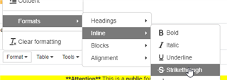
    Edit: wish there was strike-through formatting for my edit above!

  • Thanks for checking the bit state after reset. It can occasionally get more involved - I've recently learned that some internal signals can differ from their register contents based on the state of other registers, in ways that may not be straightforward to detect - as an example, the POWERDOWN bit might change the state of some internal signals, even if a particular element on the device is programmed to an active state by its register contents. Unfortunately this means the check isn't as simple as verifying register states - we likely have to look at the digital design source files to be certain there isn't a register condition, state machine trigger, or other override that we're missing.

    We do actually have a strikethrough function under the "format" menu:

    I'd definitely like to hear your feedback, as we frequently have different internal pain points than our customers - it's useful to get the outside perspective. E2E doesn't have a direct message function but I can use a friend request to give you my email where we can proceed with capturing any and all feedback you have for us.