This thread has been locked.

If you have a related question, please click the "Ask a related question" button in the top right corner. The newly created question will be automatically linked to this question.

LMX2572LP: LMX2572LP SPI configuration issue

Part Number: LMX2572LP
Other Parts Discussed in Thread: LMX2592,

Hello!
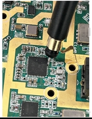
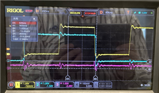
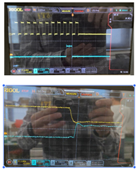
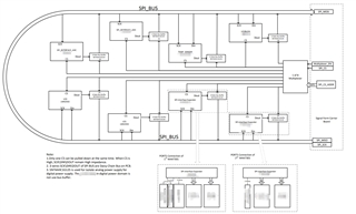
We use SPI bus to control and configure devices in system,  all devices connect to SPI bus are daisy-chain topology. There are two LMX2592 chips ,one LMX2572LP chips and other 5 devices on the SPI bus. But after configuration, only the LMX2592 and LMX2572LP were not succssfully configured, the other 5-deviecs can be configured correctly.  The read back data of LMX-devices on MUXOUT pin are all 0xFFFF. In this situation , configuration failtue is inevitable, the curve of SCK and MOSI likes this . I think the time sequence of SCK and MOSI is perfect , the voltage ringing on the rising & falling edges are in threshold of input.

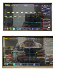
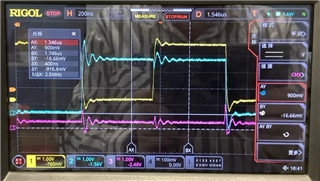
But after we only adjust the time sequece of SCK and MOSI , MOSI lag behinds SCK  20nS (20 x 1e-9 Seconds). In this situation , the LMX-devices can be stablely and  correctly configured. We have configured LMX-devices in this way for about 10K times , the LMX-devices can be successfully configured each time.
Signal CSn of two curves is LOW, CSn is correct when testing .We We used the GND ring on the probe of scope,the test point of is the pins of LMX2572LP.So I think the time delay of testing can be ignored.The "daisy-chain" is our system like this.
 
According to Timing-Charcteristics in DATASHEET , all of two sequence is OK. Why such a clock interval between SCK&MOSI can have thiis impact?
Best regards!
Leo
 
  • Hi Leo,

    I don't know why, so far we have not seen any problem is SPI programming with our programming tools - no delay between CLK and DATA. 

    Where did you probe the SPI signal? Could you probe it right next to the LMX device?

  • Hi Noel ! 

    Thank you for the reply!

    The master SPI device is a FPGA. 

    I messured the wavefoms at the pin of LMX2572LP that was compacting probe to the IC pins.Like the picture,the exposed copper is GND plane.

  • Hi Leo,

    one last thing to check, do you have 5ns or more between the falling edge of CSB and the rising edge of SCK?

  • Hi Noel!

    Sorry for replying late. 

    When retesting the wavefoms I've noticed the difference between the two situations on CSn signal.

    Pink-CSn;Blue-MOSI;Yellow-SCK.

    This curves below represents for 20ns SCK edgs to MOSI edges.

    This curves below represents for 0ns SCK edgs to MOSI edges.When the falling edges of SCK and MOSI occur simultaneously,the CSn signal exhibiting excessive jitter ,approximately 1.3V. I think this value can disabled the SPI controller.Then I think this phenomenon can cause the SPI configuration issue.

    I'll check the signal intergrity of these three-signals.

    Thank you!

    Leo