Other Parts Discussed in Thread: LMK00804B, LMK04828
Hello,
I have three queries regarding LMK00804B.
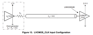
Following is the circuit I have been using to provide input from 25MHz TCXO (output impedance 200ohm typ) to the LMK00804B.
1. Can I directly connect the TCXO (LVCMOS) output with an output impedance of 200 ohm to LMK00804B LVCMOS_CLK input (pin 8) as shown below? Considering driver and transmission line impedance will be different?
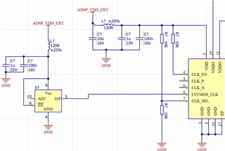
2 Or I can connect 4:1 step down BALUN at the output of TCXO (LVCMOS) and the BALUN balanced output (differential) connect to the LMK00804B buffer CLK_P and CLK_N inputs (pin5 and pin 6) as shown below?
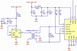
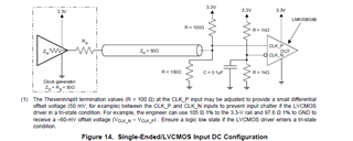
OR I should use Thevenin termination circuit as given in the datasheet (shown below) at the output of BALUN pin 1 and connect both pin 2 and 3 of BALUN to GND?
3. I need to have 2 buffered CLK output, one is for 1.8V DSP CORE CLK and other is 3.3V clock input to LMK04828 TI Clock Synth. Can I get 2 different level (1.8V and 3.3V) outputs from the same LMK00804B buffer IC or I have to use 2 LMK00804B buffer IC's to provide those two clock inputs?
Thank you,
Arshad