CDCLVC1108: logic level translation

Part Number: CDCLVC1108
Other Parts Discussed in Thread: LMK1C1108, LMK00338, LMK1D1208P

Tool/software:

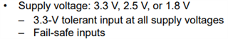
I'm trying to verify if I power the CDCLVC11xx from 2.5V (so I can get 2.5V outputs), can I drive the input with a 3.3V signal?  I assume no since the absolute maximum ratings table states input voltage max at VDD + 0.5, but I thought it was worth asking.  I'm trying to find a good level converter and 1:8 fanout buffer combination solution to replace an obsolete item.

Thank you

  • Hello Matthew,

    That is correct, the maximum Vin voltage would be 3V in this case. However, the LMK1C1108 would work, as shown in this statement from the data sheet:

    Best,

    Andrea

  • Hi Andrea,

    Thank you for the information.  I had found that part, but one thing I left out of my message was I am looking for a device without a synchronous enable input.  This is a burst clock, and I was looking at for a device to fan out clock and data signals.

    Thank you,

    -- Matt

  • Matthew,

    Note that the LMK1C is made to buffer just clocking signals and not data signals, I would recommend you use a data buffer for distributing the data.

    We do have the LMK00338 which has individual output enables for each output bank. So you can control 4 outputs with one enable, another 4 outputs with another enable, and a singular LVCMOS output with a third enable. This device is also labeled as level translator.

    Another option is the LMK1D1208P which has individual output enables and can handle 2.5V outputs with a 3.3V input. No specifics on the electrical characteristics specs but this device is not labeled as a level translator in our portfolio but I believe that it should do the trick for you.

    Best,

    Andrea