This thread has been locked.

If you have a related question, please click the "Ask a related question" button in the top right corner. The newly created question will be automatically linked to this question.

LMK03806: Programming LMK03806 and others

Part Number: LMK03806
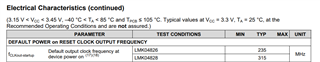
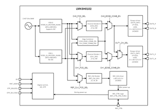
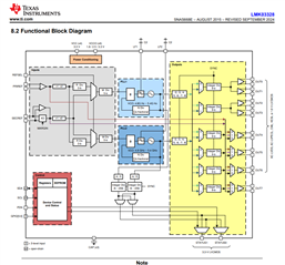
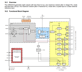
Other Parts Discussed in Thread: LMK04821, USB2ANY, LMK03318, LMK04808, LMK03328, CDCEL925, CDCE6214, CDCE913, CLOCKPRO

Tool/software:

Hi,

My question is somewhat related to my previous query:

https://e2e.ti.com/support/clock-timing-group/clock-and-timing/f/clock-timing-forum/1456461/lmk1c1104-generating-non-50-duty-cycles/5587416#5587416

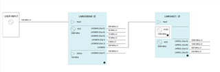
In summary I am looking for clock generators that can give me a range of clock frequencies from 2GHz (LVPECL) down to 500k (LVCMOS). I used the clock tree architect to look for suitable ICs for this purpose and the tool recommended LMK03806 and LMK04821

I plan to buy the evaluation boards for both of these ICs to test out the functionality/capability.

I have a couple of questions:

1. Should I be using something like the clock design tool (or do hand calculations suggested in AN-1865) to validate the recommendations from the clock tree architect?

2. Can I use the USB2ANY dongle for programming my end use case? I plan to take inspiration from the user guide of the eval boards for schematics design and PCB layout. However, I would like to understand if there are gotchas when trying to program multiple payloads (the 2 clock generators above) on one serial bus driven by the USB2ANY dongle.

3. Once programmed, I assume that these clock generators above remember the settings in an EEPROM, or, will I need to plan for one on the final application?

Thanks,

Prasoon

  • Prasoon,

    Would the device that you require need non-volatile memory integrated? If so, then the LMK03806 will not be suitable. Assuming that 1.8V LVCMOS is tolerated for the clock outputs, the LMK03318 can be used to generate the frequency plan shown for the LMK03806B with integrated EEPROM.

    I do not believe that we have an LMK04x device with integrated EEPROM that can be used here - I have referred this to my colleagues to comment further.

    Thanks,
    Kadeem

  • Hi Kadeem,

    My end use is a standalone application. The board deploying the clock generators would not have any host devices to configure the clock generators upon power on. 

    Thanks,

    Prasoon

  • Hi Prasoon, 
    Kadeem is correct - none of our jitter cleaners have non-volatile memory and as such a programming the IC will be required upon every power cycle. 
    Some of our older jitter cleaners do have default clocks at start up whose purpose is solely to clock a device who will then configure the jitter cleaner. 
    Take LMK04808 as an example: 

    CLKOUT4 upon POR defaults to typically a 110MHz clk which usually goes to some FPGA for example which can now configure the jitter cleaner appropriately. 

    For LMK04821 there doesn't seem to be a default clock: 

    Please note that the outputs & OSCOUT will oscillate with respect to whatever is inputted at the OSCIN pins during this time. 

    Best regards, 

    Vicente 

  • Hi Vicente,

    Thanks.

    Is there a clock generator (or multiple generators) in TI's portfolio that can give me my frequencies of interest, but, would not require a host to program the clock generator on power on?

    What about my other 2 questions? Can the USB2ANY dongle be used for programming any/all clock generators? 

    Thanks.

  • Hi Pasoon, 
    Clock tree architect is a good bet.
    If you can send your clock tree - me and Kadeem can take a long and to try and provide the best proposal that meets all your needs. 
    We would need input freq, input type, required clk outputs & formats, etc. 
    Your system requirements would also greatly help. 
    Currently - there is no device with EEPROM that can generate the frequencies shown in the snippet which are: 200,30,15,10,5,100,2000,1000,500,250MHz 

    In regard to the USB2ANY dongle - most our EVMs include this device for communication/programming. 
    Please try to connect one USB2ANY at a time otherwise TICSpro can get a bit buggy. 

    Some devices already have an MSP430 MCU on board and thus don't shit with the grey box USB2ANY dongle or in other words, they already have USB2ANY on board and simply require a USB cable. 

    What I'm thinking we can utilize a device like LMK03318 which contains EEPROM to create most of the LVCMOS clocks and then we can input those clocks into another LMK03318 for the higher frequency outputs. Are those frequencies fixed or can they be adjusted? 

    Best regards, 

    Vicente 

  • Thanks Vicente. I can send you my requirements. Should I just post them here? Or, I can send out a slide deck capturing the requirements to an email address.

    Prasoon

  • If you're concerned about posting on this public forum - you can email me at v-floresprado@ti.com
    If you have no concerns, you can also post here - usually easier to follow as well. 
    Emails tend to get lost sometimes. 

    Best regards,

    Vicente 

  • Hi Vicente,

    I have captured the requirements on the attached slide. 

    Thanks.

    Clock requirements.pptx

  • Hi Prasoon, 
    It seems like LMK3H210x + LMK03318 is the best solution which meets your needs. 
    They're a few requirements that are a bit difficult to implement though. 
    Such as the fixed phase relationship between Input & Ouput but using a XTAL as source. 

    LMK3H210x utilizes our BAW technology instead of requiring a ref clk. 

    I have attached the block diagram of the two-output version. 

    For your application a 4 or 8 output variant (sampling soon if i'm not wrong Kadeem/Cris pls correct me if i'm wrong) would be required. 

    LMK3H210x utilizes one-time programmable (OTP) memory and LMK03318 uses EEPROM so you will not need to configure these devices upon every power cycle. 
    The idea is for the LMK3H210x to create the LVMCOS clocks with a 200MHz FOD and the LMK03318 generating the higher frequency LVPECL clocks. 


    I have added our clock gen AE in case you have configuration questions. 
    Do you have any power consumption requirements or jitter requirements? Given you mention you drive transmission line test structures I would want to presume jitter isn't a cause for concern but rather drive strength or slew rate? 

    Best regards, 

    Vicente 

  • Hi Vicente,

    Thanks for the information.

    I started looking at the data sheet for LMK3H210x. Does the OTP feature need to be programmed at TI, or, is it user programmable?

    The 4 or 8 output variants of this clock generators are coming to market soon?

    Can 2x of LMK03318 be used for this application? Or, is the VCO frequency too high to drive the lower LVCMOS frequencies?

  • Hi Prasoon,

    I will let Cris or Kadeem comment on the exact date but it should be this year I think - don’t quote me though. 

    TI needs to program OTP if you don’t desire to use the default configuration - which is the case for your application.

    You can use 2 LMK03318 but the issue now becomes you need an external ref clk, usually an XO to drive the first clk gen.

    LMK3H210x eliminates needing a third component since BAW is inside.

    Best regards,

    Vicente

  • Hi Vicente,

    Thanks.

    End of the year (worse case) maybe a bit late for my application. I am trying to get something in-hand in the next 2-3 months.

    I did some research (on Google) and XOs are recommended for their superior temperature/phase stability over SAW/BAW devices. Since my application is along the lines of metrology, I desire this stability. I may even end up using a temperature compensated XO for this.

    "You can use 2 LMK03318 but the issue now becomes you need an external ref clk, usually an XO to drive the first clk gen."

    Are you saying this because, I asked for fewer components? I may need to enable power gating or output disabling on my board to keep power low

    Looks like needing to use 2 different clock generators is inevitable. Can both of them share the same USB2ANY bus? I am thinking about the SPI headers shown in the schematic for LMK04821EVM:

    https://www.ti.com/lit/ug/snau168/snau168.pdf?ts=1736985354428&ref_url=https%253A%252F%252Fwww.ti.com%252Ftool%252FLMK04821EVM

    and connecting both clock generators (2x of LMK03318) to this bus?

    Prasoon

  • Hi Prasoon, 
    I understand BAW is pretty stable overall. 

    https://www.ti.com/lit/an/snaa362/snaa362.pdf?ts=1737072257781&ref_url=https%253A%252F%252Fwww.ti.com%252Fproduct%252FLMK6P

    I can loop in our Oscillator expert as well if you need help comparing. 
    The USB2ANY bus varies. 
    The LMK04821 utilizes SPI to communicate/control the device. 
    LMK03318 uses I2C. 

    LMK3H210x uses I2C as well. 
    As long as we have different I2C addresses for both devices they can be on same bus. 


    Best regards, 

    Vicente 

  • Hi Vicente,

    LMK03318 can only go upto 1000MHz, looks like.

    Regards,

    Prasoon

  • Prasoon,

    Sorry for the extended delay in my responses, I have been on business travel.

    For generating the 2000MHz clock, the LMK033x8 devices cannot support this. The only devices in the portfolio that support this are the LMX devices or the jitter cleaner devices, both not having EEPROM. Generating this frequency will require support of a programming interface. Otherwise, LMK03328 is suitable for the remaining clocks from a single device leveraging one of the status pin outputs (3.3V LVCMOS).

    Thanks,

    Kadeem

  • Thanks Kadeem.

  • Hi Kadeem,

    Perhaps I am missing something here.

    LMK03328 still provides upto 8 output banks. It does have 1 extra PLL module. But the number of outputs is still the same as LMK03318. Am I missing something? I do get the advantage of optimizing with 2 different VCOs, but, the total number of outputs is still the same:

    Thanks 

    Prasoon

  • Hi Kadeem/Vicente,

    I have done some rough calculations for 2 solutions: LMK03318 + LMK03318 and LMK03318 + CDCEL925. I think the LMK03318 + CDCEx925 hits more of the check boxes, assuming closed loop operation is achieved for both

    Solution

    Dev Model fin VCO1 Post PLL Divide Out0 Out1 Out2 Out3 Out4 Out5 Out6 Out7 Status0/Status1
    2x LMK03318 LMK03318 XTAL 5000 5 Integer Div 5 5 10 10 1 2 4 100 1250
    Out freq 200 200 100 100 1000 500 250 10 4
    Out Type 1.8V LVCMOS 1.8V LVCMOS 1.8V LVCMOS 1.8V LVCMOS LVPECL LVPECL LVPECL 1.8V LVCMOS 3.3V LVCMOS
    Comments Meets Spec Meets Spec/disable if not needed Meets Spec Meets Spec/disable if not needed Meets Spec Meets Spec Meets Spec Also useful for debug by re-directing ref input out Lowest integer possible
    Dev Model fin VCO1 Post PLL Divide Out0 Out1 Out2 Out3 Out4 Out5 Out6 Out7 Status0/Status1
    LMK03318 100M, LVCMOS above 4800 8 Integer Div 256 256 256 256 20 40 120 240 1250
    Out freq 2.34375 2.34375 2.34375 2.34375 30 15 5 2.5 3.84
    Out Type 1.8V LVCMOS 1.8V LVCMOS 1.8V LVCMOS 1.8V LVCMOS 1.8V LVCMOS 1.8V LVCMOS 1.8V LVCMOS 1.8V LVCMOS 3.3V LVCMOS
    Comments Lowest possible/does not meet spec Lowest possible/does not meet spec Lowest possible/does not meet spec Lowest possible/does not meet spec Meets Spec Meets Spec Meets Spec Also useful for debug by re-directing ref input out Lowest integer possible
    Y1 Y2 Y3
    LMK03318 + CDCEL925 Dev Model fin PLL1/VCO1 (N,M) Pdiv (1-127) 4 8 24
    CDCEL925 100 M, LVCMOS 120 (120,10) Out Freq 30 15 5
    (240,20) Out Type 1.8V LVCMOS 1.8V LVCMOS 1.8V LVCMOS
    Comments Meets Spec Meets Spec Meets Spec
    Y4 Y5
    PLL2/VCO2 (N,M) Pdiv (1-127) 40 80
    80 (8,10) Out Freq 2 1
    (16,20) Out Type 1.8V LVCMOS 1.8V LVCMOS
    (4,5) Comments Meets Spec Meets Spec, lowest possible is 80/127 = 0.63 M

    I think there is some headroom in fvco in CDCEx925 for the lower frequencies.

    What do you think?

  • Prasoon,

    This is correct for the CDCEx925. Potentially the CDCE6214 may have better flexibility for generating lower-frequency outputs, but the tradeoff here is that only 2 LVCMOS output frequencies + a copy of the input frequency are available.

    Thanks,

    Kadeem

  • Hi Kadeem,

    Thanks for the suggestion. I think I am going to stick with the CDCEx925. 

    Both LMK03318 and CDCEx925 can be on the same I2C bus for EEPROM programming, am I correct?

    Thanks.

  • I meant to ask if both of these can be on the same I2C bus and be programmable with the USB2ANY dongle?

    Thanks.

  • Prasoon,

    These can both be on the same I2C bus. However, the software for interfacing with each is different and requires different hardware. LMK033x8 can be programmed using TICS Pro with the USB2ANY, which is straightforward. For the CDCE913, you will have to determine the registers to write using ClockPro, but leverage the USB2ANY Explorer to manually perform the I2C writes. The ClockPro software is not compatible with the USB2ANY.

    Thanks,

    Kadeem