LMK04821: LMK04828 phase synchronization issue between multiple boards

Part Number: LMK04821
Other Parts Discussed in Thread: LMK04828

Tool/software:

Hi Teams,

The customer now wants to achieve phase synchronization between the output clocks of LMK04828 between multiple boards, with phase always randomly changing. They have also referred to documents that can be found on the forum, but the clock architecture of their hardware may be slightly different and cannot be fully replicated; Can you provide us with some assistance?

This is their hardware architecture, with OSCin outputting a 125M clock.

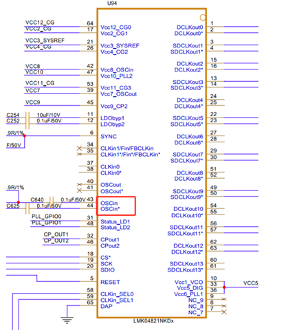
The actual customer is currently using LMK04828B, which is only compatible on the schematic and has not been updated.

This is the register configuration used by the customer for single board multi-channel clock synchronization previously generated through software

R0 (INIT)	0x000090
R0	0x000010
R2	0x000200
R3	0x000306
R4	0x0004D0
R5	0x00055B
R6	0x000600
R12	0x000C51
R13	0x000D04
R256	0x010014
R257	0x010155
R258	0x010255
R259	0x010301
R260	0x010422
R261	0x010500
R262	0x010670
R263	0x010766
R264	0x010814
R265	0x010955
R266	0x010A55
R267	0x010B01
R268	0x010C22
R269	0x010D00
R270	0x010E70
R271	0x010F66
R272	0x011008
R273	0x011155
R274	0x011255
R275	0x011301
R276	0x011422
R277	0x011500
R278	0x011670
R279	0x011760
R280	0x011818
R281	0x011955
R282	0x011A55
R283	0x011B01
R284	0x011C22
R285	0x011D00
R286	0x011E70
R287	0x011F10
R288	0x012008
R289	0x012155
R290	0x012255
R291	0x012301
R292	0x012422
R293	0x012500
R294	0x012670
R295	0x012710
R296	0x012808
R297	0x012955
R298	0x012A55
R299	0x012B01
R300	0x012C22
R301	0x012D00
R302	0x012E70
R303	0x012F60
R304	0x013006
R305	0x013155
R306	0x013255
R307	0x013301
R308	0x013422
R309	0x013500
R310	0x013671
R311	0x013701
R312	0x013800
R313	0x013903
R314	0x013A03
R315	0x013B00
R316	0x013C00
R317	0x013D08
R318	0x013E01
R319	0x013F00
R320	0x014081
R321	0x014100
R322	0x014200
R323	0x014311
R324	0x0144FF
R325	0x01457F
R326	0x014608
R327	0x01471F
R328	0x014802
R329	0x014942
R330	0x014A02
R331	0x014B16
R332	0x014C00
R333	0x014D00
R334	0x014EC0
R335	0x014F7F
R336	0x015003
R337	0x015102
R338	0x015200
R339	0x015300
R340	0x015478
R341	0x015500
R342	0x015678
R343	0x015700
R344	0x015896
R345	0x015900
R346	0x015A0A
R347	0x015BD4
R348	0x015C20
R349	0x015D00
R350	0x015E00
R351	0x015F0B
R352	0x016000
R353	0x016104
R354	0x016224
R355	0x016300
R356	0x016400
R357	0x01650C
R369	0x0171AA
R370	0x017202
R380	0x017C15
R381	0x017D33
R358	0x016600
R359	0x016700
R360	0x016828
R361	0x016959
R362	0x016A20
R363	0x016B00
R364	0x016C00
R365	0x016D00
R366	0x016E13
R371	0x017300
R386	0x018200
R387	0x018300
R388	0x018400
R389	0x018500
R392	0x018800
R393	0x018900
R394	0x018A00
R395	0x018B00
R8189	0x1FFD00
R8190	0x1FFE00
R8191	0x1FFF53

Please help  take a look at this issue, thank you~

  • Hi Vayne, 

    Can you share how you are phase synchronizing the LMK04828 outputs on the different boards? Based on your schematic, it appears your CLKin0 is unused, and could be better suited for a shared SYNC pulse across different boards (the pulse must arrive to both boards within the same 400ps window, based on your VCO frequency) - for more information, visit this link.

    Alternatively, if your boards have a common input reference, configuring the device in nested ZDM would allow for a much easier method of ensuring a shared phase determinism to the reference across the outputs of different boards. A SYNC event would still be necessary, but there is no time limitation since the outputs will all be aligned to the looped back output.

    Thanks,

    Michael

  • Hi Michael,

    The 125M input is provided by another module on each board, and the modules are connected through a switch to ensure that the 125M reference clock input is from the same source and synchronized; Regarding the synchronization between multiple boards, the customer's solution is to send a pulse through the sync pin to achieve synchronization. The specific method is to send a trigger signal to both boards simultaneously through an external signal source. When this signal is detected by the FPGA, a enable is raised. During the effective period of the enable, when the 1pps signal sent by the 125M clock module is detected, the two signals will be synchronized with each other in the logic. The new signal after the phase is used as the synchronization event for 04828 in the multiple boards.

    They referred to the document you provided, and the customer now has the condition to send synchronization events to two board cards through sync pins at the same time (time accuracy should not reach ps level). The above also specifically describes the process of sending synchronization events through sync pins. In the second solution you provided, the customer seems to be able to achieve phase synchronization between multiple board cards (with relative phase remaining unchanged). They want to know the specific register configuration.thank you!

  • Hi Vayne,

    Attached is the register configuration (both as a .tcs and a .txt file) for single loop ZDM. 

    R0 (INIT)	0x000090
    R0	0x000010
    R2	0x000200
    R3	0x000306
    R4	0x0004D0
    R5	0x00055B
    R6	0x000600
    R12	0x000C51
    R13	0x000D04
    R256	0x010014
    R257	0x010155
    R258	0x010255
    R259	0x010301
    R260	0x010422
    R261	0x010500
    R262	0x010670
    R263	0x010766
    R264	0x010814
    R265	0x010955
    R266	0x010A55
    R267	0x010B01
    R268	0x010C22
    R269	0x010D00
    R270	0x010E70
    R271	0x010F66
    R272	0x011008
    R273	0x011155
    R274	0x011255
    R275	0x011301
    R276	0x011422
    R277	0x011500
    R278	0x011670
    R279	0x011760
    R280	0x011818
    R281	0x011955
    R282	0x011A55
    R283	0x011B01
    R284	0x011C22
    R285	0x011D00
    R286	0x011E70
    R287	0x011F10
    R288	0x012008
    R289	0x012155
    R290	0x012255
    R291	0x012301
    R292	0x012422
    R293	0x012500
    R294	0x012670
    R295	0x012713
    R296	0x012808
    R297	0x012955
    R298	0x012A55
    R299	0x012B01
    R300	0x012C22
    R301	0x012D00
    R302	0x012E70
    R303	0x012F60
    R304	0x013006
    R305	0x013155
    R306	0x013255
    R307	0x013301
    R308	0x013422
    R309	0x013500
    R310	0x013671
    R311	0x013701
    R312	0x013800
    R313	0x013903
    R314	0x013A03
    R315	0x013B00
    R316	0x013C00
    R317	0x013D08
    R318	0x013E01
    R319	0x013F13
    R320	0x014081
    R321	0x014100
    R322	0x014200
    R323	0x014311
    R324	0x0144FF
    R325	0x01457F
    R326	0x014608
    R327	0x01471F
    R328	0x014802
    R329	0x014942
    R330	0x014A02
    R331	0x014B16
    R332	0x014C00
    R333	0x014D00
    R334	0x014EC0
    R335	0x014F7F
    R336	0x015003
    R337	0x015102
    R338	0x015200
    R339	0x015300
    R340	0x015478
    R341	0x015500
    R342	0x015678
    R343	0x015700
    R344	0x015896
    R345	0x015900
    R346	0x015A0A
    R347	0x015BD4
    R348	0x015C20
    R349	0x015D00
    R350	0x015E00
    R351	0x015F0B
    R352	0x016000
    R353	0x016104
    R354	0x016224
    R355	0x016300
    R356	0x016400
    R357	0x016528
    R369	0x0171AA
    R370	0x017202
    R380	0x017C15
    R381	0x017D33
    R358	0x016600
    R359	0x016700
    R360	0x01680A
    R361	0x016959
    R362	0x016A20
    R363	0x016B00
    R364	0x016C00
    R365	0x016D00
    R366	0x016E13
    R371	0x017300
    R386	0x018200
    R387	0x018300
    R388	0x018400
    R389	0x018500
    R392	0x018800
    R393	0x018900
    R394	0x018A00
    R395	0x018B00
    R8189	0x1FFD00
    R8190	0x1FFE00
    R8191	0x1FFF53
    

    lmk04828_zdm_singleloop.tcs

    Thanks,

    Michael