This thread has been locked.

If you have a related question, please click the "Ask a related question" button in the top right corner. The newly created question will be automatically linked to this question.

LMK04610EVM: USB2ANY Programmer pin number mismatch and voltage level

Part Number: LMK04610EVM
Other Parts Discussed in Thread: LMK04610, USB2ANY,

Hi,

The clock tree design for the system is planning to be implemented with LMK04610. The Kintex FPGA on board will configure the LMK04610.
But the option for programming LMK04610 with USB2ANY is also incorporated for easy debugging.

Please have a look at the doubts that follows

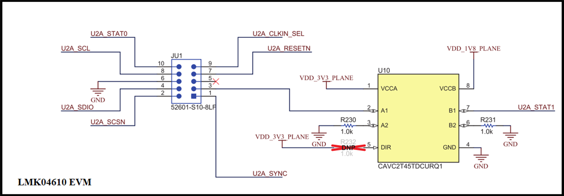
Q1. Why the level shifter CAVC2T45TDCURQ1 is connected between USB2ANY and LMK04610? Why is it given only on the STATUS1 pin and not in STATUS0 pin?


Q2. What is the voltage level of the signals available in the USB2ANY connector? Please validate the following
    Pin 1= SYNC= 1.8V
    Pin 2= SCSN= 3.3V
    Pin 3= STATUS1= 3.3V
    Pin 4= SDIO= 1.8V
    Pin 5= NC
    Pin 6= GND
    Pin 7= RESETN= 3.3V
    Pin 8= SCL= 3.3V
    Pin 9= CLKIN_SEL= 1.8V
    Pin 10= STATUS0= 1.8V

Q3. The FRC-10 pin cable from USB2ANY adaptor is connected to the socket JU1 on the Evaluation board of LMK04610.
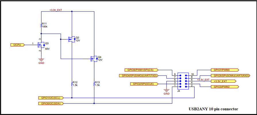
   From the schematic of USB2ANY (J4 on SNAU228) the 'pin6 is External 3.3V' and 'pin5 is ground' but it doesn't suit with the
   pin mapping of JU1 connector on LMK04610 EVM as it has 'pin5 as NC' and 'pin6 as the ground'.
   Both images are attached here.
   That results in two things 'lack of common ground' and 'shorting of 3.3V supply inside USB2ANY'.
   But it still working in EVM...
   Do my observation are right? Elsewhere I miss the train?


Q4. If I adopt the same USB2ANY connection part with 'JU1 and CAVC2T45TDCURQ1' in my schematic, Can I use the USB2ANY module for programming the LMK04610 or is there anything more to keep in mind.

Thanks in advance
DEEPAK V

  • Hello DEEPAK V,
    about your questions:
    Q1: The USB2ANY box shipped with the EVM is 3.3V only signals. The status pins are part of the 1.8V domain. The USB2ANY box offers internally a 4-wire SPI while the LMK04610 can provide 4-wire SPI or 3-wire SPI. That is why we only put a level shifter on one pin to allow reading back into the GUI.

    Q2: The USB2ANY box only provides 3.3V levels. The voltage dividers sit on the EVM. Please look at page 29 of the user guide www.ti.com/.../snau201a.pdf

    Q3: These are two different connectors on two different boards. They are not the same connector. They fit together.

    Q4: As mentioned above, when you do that please be aware to also re-use the voltage dividers respectively. You may want to place the different pull-up/pull-down options so that you can use the pin functions at power-up (e.g. OSCout divider). I also recommend to put a pull-up for RESETN, so that you can disconnect the cable without disturbing device operation.

    Best regards,
    Patrick
  • Hi Patrick,

    Thank you for answering my queries. Now I have understood more about LMK04610EVM.

    But still few more doubts persists, Please have a look at the following

    Q1: The level shifter CAVC2T45TDCURQ1 is meant to support reading back SPI configuration information from LMK04610 to the GUI.
    But the Direction pin (DIR) of the level shifter is not connected to ground, 'it is floating' OR 'it can be connected to VCC' when the resistor(1K) is populated.
    In both cases, the data transfer can't happen from Port B(1.8V side) to Port A(3.3V side). For reading back data have to transfer from Port B to Port A.
    Then how the read back will work?

    Q2: Based on your suggestion I have gone through the page 29 of EVM and found voltage dividers for SCSN, SCL, STATUS1, STATUS0, SYNC and RESETN.
    But unable to find voltage dividers for signals SDIO and CLOCKIN_SEL. Both of them have default switch position as 2 (U2A Signal) which has an only 4.7K
    series resistor in the path and hence 3.3V signals are coming directly to SDIO & CLOCKIN_SEL.Please help me to find where my observations went wrong?

    Q3. To continue the system operation without disturbance after USB2ANY cable removal, a pull-up resistor is being placed in our schematic on
    the RESETN pin based on your suggestion. But datasheet recommended to keep REST to Ground during the power supply ramping time,
    but this will be violated if we keep the pull-up. Can we discard this information and follow with the pull-up?

    Q4. Do any digital control/interfaces pins have internal pull-up or pull-down?

    Q5. Is it compatible to use USB2ANY adaptor shipped with some other EVM with LMK04610 Evaluation Board.

    Thanks once again for continuing support.

    Thanks and regards
    DEEPAK V

  • Hello DEEPAK V,
    you are welcome!
    About your new questions:
    Q1: It is correct, the DIR pin must see a logic low level so that the transfer happens in the correct direction. When the pin is left floating it still has some weak connection to GND, so for our EVM this is working. For an application I recommend you use an actual pull-down resistor.
    Q2: We saved some additional components: CLKIN_SEL R170 + R146 via the DIP switch. Similar for SDIO R168 + R143.
    Q3: Sorry, for not clarifying: The pull-up on our EVM can be set optionally. This means when I have a sensitive measurement and I want to disconnect the PC (=USB2ANY), then I place the jumper to have the pull-up. In application this might mean you have to control the timing through an MCU or connect a capacitor to delay the signal. Maybe you already have a supply IC which provides a "power good" signal?
    Q4: Yes, these options exist inside the LMK04610 pins. They are deactivated by default and have to be enabled manually.
    Q5: Yes, when you have an USB2ANY from another clocking EVM this will work fine with the LMK04610EVM. It only may happen that for the TICS Pro software a firmware update of the USB2ANY may be required. (which will happen automatically when you connect it)

    Best regards,
    Patrick