This thread has been locked.

If you have a related question, please click the "Ask a related question" button in the top right corner. The newly created question will be automatically linked to this question.

LMK04616: SYSREF SPI trigger problem

Part Number: LMK04616
Other Parts Discussed in Thread: LMK04828

Hi all,

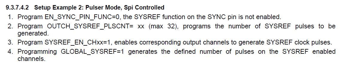
Using a LMK04616 I need to issue a SYSREF using a SPI trigger, but very frequently the SYSREF signal is not generated after the trigger. 

The following is the sequence performed, after which we trigger the SYSREF writing 0x14 = 10.

0x140 = 0x1
0x14E = 0x0
0x128 = 0x25
0x129 = 0x25
0x14 = 0x01
0x14 = 0x00
0x128 = 0x5
0x129 = 0x5
0x14E = 0x6
0x14 = 0x10

does anyone have an idea ?
Maxx

  • Can you share your TICS Pro config file (initialization settings prior to SYSREF programming), schematic, and VCXO spec, so these can be reviewed?

    Alan
  • Hi Maxx,

    The problem could be caused by 0x14 settings.

    Refer to below example.


    Regards,

    Shawn

  • Hi, in attach the configuration files, init, SYSREF and trigger.

    PS: if I force continuos mode the output is correct

    Maxx

    //////////////////////////////////////////////////////////////////////77

    mnt_pll_io_init();

    Wait_us(5);

    // 9.5 Programming
    // LMK0461x device is programmed using 24-bit registers.
    // Each register consists of a 1-bit command field (R/W), a 15-bit address field (A14 to A0)
    // and a 8-bit data field (D7 to D0).
    // The contents of each register is clocked in MSB first (R/W), and the LSB (D0) last.
    // During programming, the CS* signal is held low.
    // The serial data is clocked in on the rising edge of the SCK signal.
    // After the LSB is clocked in, the CS* signal goes high to latch the contents into the shift register.
    // TI recommends programming registers in numeric order -- for example, 0x000 to 0x1FFF --
    // to achieve proper device operation.
    // Each register consists of one or more fields that control the device functionality.
    // See the electrical characteristics and Figure 1 for timing details.
    // R/W bit = 0 is for SPI write. R/W bit = 1 is for SPI read.

    // 9.5.1 Recommended Programming Sequence
    // The default programming sequence from POR involves:
    // 1. Toggle RESETn pin High-Low-High
    mnt_pll_rst_out();
    Wait_us(50);
    mnt_pll_rst_in();
    Wait_us(50);
    mnt_pll_rst_out();
    Wait_us(500000);

    // 2. Program all registers with Register 0x0011 bit 0 = 0
    val = 0x00;
    mnt_pll_byte_io(LMK04616_WR, 0x0011, &val);
    // lmk04616_reg_wr(0x0011, val);
    // mnt_pll_byte_io(LMK04616_RD, 0x0011, &val);
    // Wait_us(20);

    for (i = 0; i < LMK04616_REG_NUM; i++) {
    val = regs_array[i] & 0xFF;
    mnt_pll_byte_io(LMK04616_WR, (regs_array[i] >> 8), &val);
    // lmk04616_reg_wr((regs_array[i] >> 8), val);
    // Wait_us(20);
    // mnt_pll_byte_io(LMK04616_RD, (regs_array[i] >> 8), &val);
    }

    // 3. Program Register 0x0011 bit 0 = 1
    val = 0x01;
    mnt_pll_byte_io(LMK04616_WR, 0x0011, &val);
    // lmk04616_reg_wr(0x0011, val);
    // mnt_pll_byte_io(LMK04616_RD, 0x0011, &val);

    Wait_us(20);
    //
    // val = 0xFF; // Prevent all output from becoming synchronized during a SYNC
    // mnt_pll_byte_io(LMK04616_WR, 0x144, &val);

    // Wait_us(500);
    //
    // val = 0x12; // Enables the SYNC functionality -
    // // SYNC event generated from SYNC pin or if enabled the SYNC_PLL1_DLD flag or SYNC_PLL2_DLD flag.
    // mnt_pll_byte_io(LMK04616_WR, 0x143, &val);
    // mnt_pll_byte_io(LMK04616_RD, 0x143, &val);

    // Wait_us(500);

    // tutto acceso
    // lmk04828_reg_wr(0x140, 0x00); DAFA PCIEXJESD

    // Wait_us(500);

    for(i = 0; i < 8; i++) {
    val = 0x00;
    mnt_pll_byte_io(LMK04616_RD, (0x00127 + i), &val);

    val |= 0x20;
    mnt_pll_byte_io(LMK04616_WR, (0x00127 + i), &val);
    }

    val = 0x01;
    mnt_pll_byte_io(LMK04616_WR, 0x0014, &val);

    Wait_us(500);

    val = 0x00;
    mnt_pll_byte_io(LMK04616_WR, 0x0014, &val);

    Wait_us(500);

    // mnt_pll_sysref_req(); // sync event
    val = 0x10;
    mnt_pll_byte_io(LMK04616_WR, 0x0014, &val);
    // lmk04616_reg_wr(0x0014, val);
    // mnt_pll_byte_io(LMK04616_RD, 0x0014, &val);

    Wait_us(500);

    return 0;
    }

    /*******************************************************************************
    *
    * FUNCTION : mnt_pll_sysref_req
    * PURPOSE : //M@B richiesta sysref
    * PARAMETERS : //M@H nessuno
    * RETURN VALUES :
    * SPECIFICATION :
    */
    void /*M@F*/ mnt_pll_sysref_req(void)
    {
    uint8_t val;

    val = 0x10;
    mnt_pll_byte_io(LMK04616_WR, 0x0014, &val);

    Wait_us(5);
    }

    ticsXti.zip

  • How about to generate 32 SYSREF pulses ?
  • Note that when you wrote Register 0x0014, you write SYNC_PIN_FUNC[1:0] bits to 00b, but this should be 10b for Sysref Request. Per 9.3.7.4, program Register 0x0140 to 0x20 (OUTCH_SYSREF_PLSCNT = 32 pulses) before writing to Register 0x0014 to 0x12 (GLOBAL_SYSREF=1 and SYNC_PIN_FUNC[1:0]=01b).

    Alan