This thread has been locked.

If you have a related question, please click the "Ask a related question" button in the top right corner. The newly created question will be automatically linked to this question.

LKM04616

Part Number: LMK04616
Other Parts Discussed in Thread: DAC38RF83, , LMX2594

Hi, 

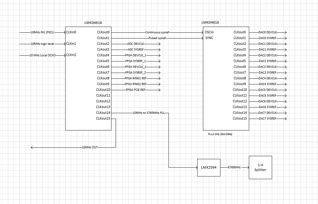
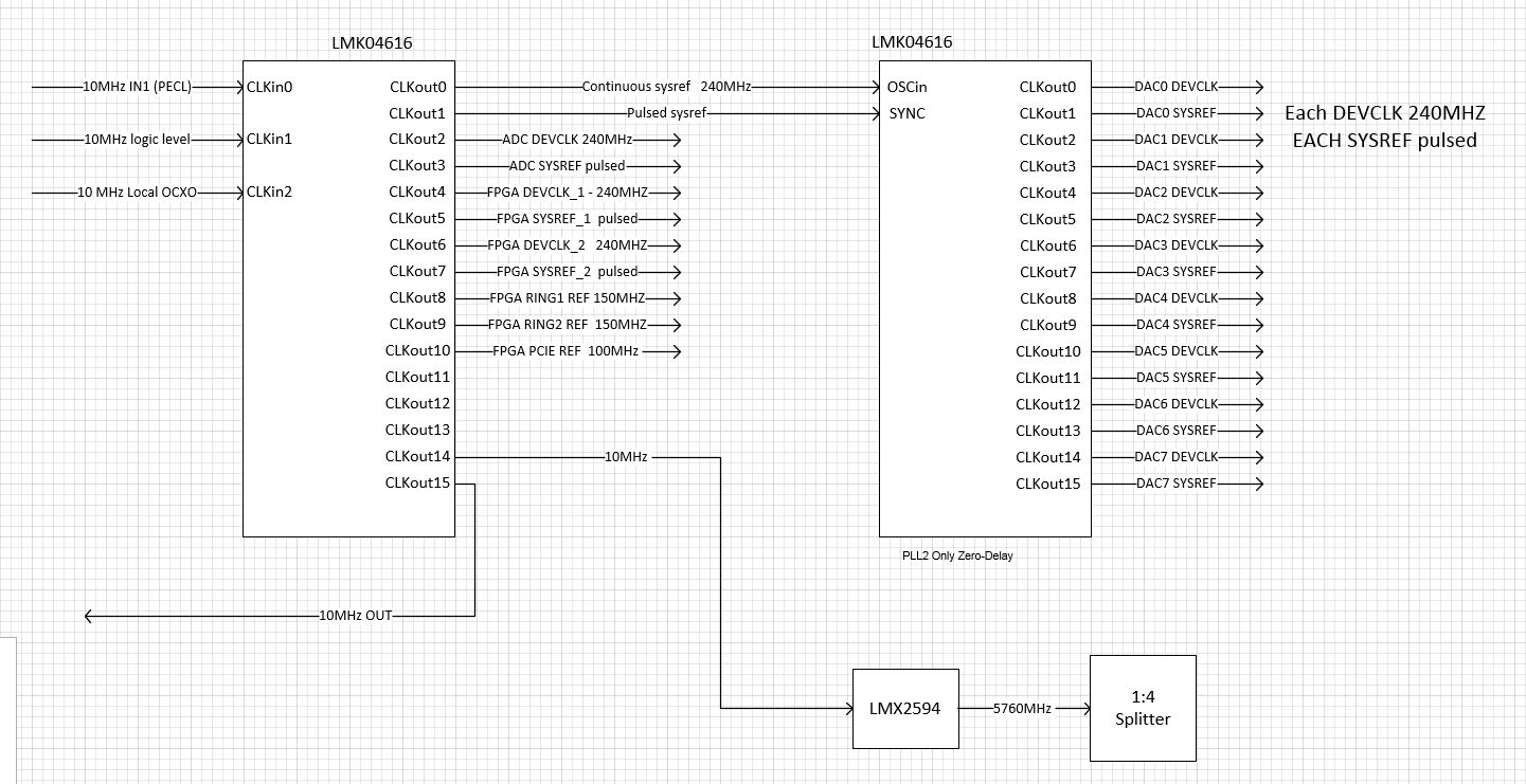
I have attached a block diagram of what I intented to design .

Can someone review it?

I need to connect 8 DAC38RF83 with JESD204B.

The first LMK04616 is PLL2 only and the FPGA will pick the input CLK ( 1 of 3).

the second LKM04616  all the DEVCLK and SYSREF are match lenght.( need to transmut from the dacs at phase align) 

  • Hello Shlomi,

    Placing a continuous clock on the same group as a pulsed clock as with CLKout0/1 in this diagram is not possible. When SYSREF_EN_CHx_y is asserted, both channels are held low until a SYSREF request is generated or GLOBAL_CONT_SYSREF is asserted. Continuous clocks should be on a separate output grouping from pulsed clocks. If both continuous SYSREF and pulsed SYSREF are required, continuous SYSREF should just be treated as a regular continuous clock.

    What are the frequencies required for each of those outputs? Every clock must be derived from the VCO post-divider output, which can make some values difficult to hit without careful frequency planning.

    Regards,

  • Hi Derek,

    I added the freq to the block. how I need to arrange it?

  • Thanks Shlomi,

    I suggest the following:

    CLKout0: 240 MHz continuous OSCin SYSREF
    CLKout1: 240 MHz ADC DEVCLK

    CLKout2: 240 MHz pulsed SYNC pin SYSREF
    CLKout3: 240 MHz pulsed ADC SYSREF

    CLKout4: 240 MHz FPGA DEVCLK_1
    CLKout5: 240 MHz FPGA DEVCLK_2

    CLKout6: 240 MHz pulsed FPGA SYSREF
    CLKout7: 240 MHz pulsed FPGA SYSREF

    CLKout8: unused (lower crosstalk)
    CLKout9: unused (lower crosstalk)

    CLKout10: 150 MHz FPGA RING1 REF
    CLKout11: 150 MHz FPGA RING2 REF

    CLKout12: unused
    CLKout13: 10 MHz OUT

    CLKout14: 100MHz LMX2594
    CLKout15: 100MHz FPGA PCIE REF

    This accomplishes several objectives:

    • All continuous clocks are grouped, and all pulsed clocks are grouped. If a pair of grouped pulsed SYSREF outputs need to be independently requested, the unwanted output can be temporarily powered down at the output buffer.
    • Some crosstalk isolation from the 240 MHz, 150 MHz, and 100 MHz signals
    • I suggest increasing the LMX2594 clock to 100 MHz to take advantage of the high phase detector frequency. On the other hand, this may introduce unwanted fractional spurs; in that case, put the 100MHz FPGA clock on CLKout12/13 and group the 10MHz on CLKout14/15.

    If you need to rearrange the output locations on the LMK04616 to simplify layout, that should be fine as well. Just make sure to move them in the pairs listed above.

    I also checked the frequencies, and you should be able to achieve every listed frequency with a VCO frequency of 6000MHz and a post divider of 5.