


The THS788 seems to be outputting 23 bits plus the tag bit per strobe vs. the expected 24 bits plus the tag bit in the 24 bit Result Transfer Format. I have attached a bmp showing the scope output in both modes (cut&paste overlayed). This problem was discovered as our device would occasionally power up in the erroneous state. As the FPGA was expecting to shift in 24 bits but only received 23 bits the timestamp for the samples appeared to be multiplied by 2. I can reproduce the problem now by executing a power down, power up, reset and configure sequence over the host bus. The FPGA configuration stays constant through this sequence. By doing this multiple times during the same power on period the THS788 seems to get into the 23 bit error state about 1 in 7 times. I would be happy to provide TI with the C source function from our firmware responsible for the configuration of the TDC over the host bus but would like to do so in a private email.
Host Bus Frequency: 40 MHz
Result Bus Frequency: 150 MHz
Result Bus in DDR mode
Thanks very much for any help you can provide with this.
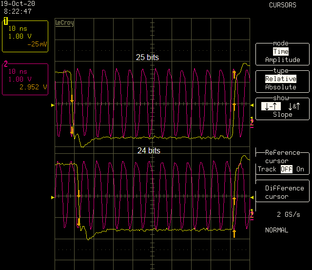
Red waveform is RClk
Yellow waveform is strobe.
Both signals are routed through our FPGA and then out to testpoints. We're not clocking the strobe before routing it to the testpoint but there is a LVDS to single-ended conversion occuring. The rClk is converted from LVDS to single ended within the FPGA and is then connected to a DDR output I/O register. On the rising edge of the clock the DDR register outputs a high, on the falling edge it outputs a low (so should mirror the clock without our actually routing the clock to an IO pin).
