This thread has been locked.

If you have a related question, please click the "Ask a related question" button in the top right corner. The newly created question will be automatically linked to this question.

LMK04826: Multi LMK Synchronization -- Using LMK Sync Pin

Part Number: LMK04826
Other Parts Discussed in Thread: DAC38J84, , LMK04828

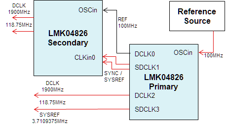
We are using three LMK04826B on our custom board. We are giving input of fixed 100 MHz to OSCin to three LMK's.
The following clocking scheme is implemented.


We are using VCO of 1900MHz and generate required clock for both FPGA and Dac38j84.
Dac clock     - 1900 MHz
Sysref          - 3.7109375 MHz
FPGA clock - 118.75MHz

In order to get clock and sysref aligned between multiple LMKs. We are generating a single pulse from FPGA and passing over sync pin of all the LMK's


1. Trace Lengths between FPGA -- LMK 1, FPGA  -- LMK 2, FPGA -- LMK 3 are not same.

By monitoring the SYNC pin of LMK 1 and LMK 2, the delay between the pulses is 120 ps. We are using SYNC_1_shot_EN.

When we are monitoring the LMK 1 and LMK 2 Sysref outputs, they are alligned with zero delay.

It is difficult to monitor 1900 MHz clock between LMK 1 and LMK 2, So we went for device clock of 475 MHz. At 475 MHz, Delay between LMK 1 and LMK 2 is 320 ps. It is same across multiple power cycles.

If Sysref are aligned perfectly, why there is delay at Device clocks ??

Is it required to maintain same Trace lengths between (SYNC pins -- FPGA ) for all LMK's ??

2. If they are not length matched, What is the minimum skew that LMKs can adjust to synchronize the outputs of different LMK's.

3. Is it required to give SYNC Synchronous to the LMK Input Clock ??


4. Same SYNC is used for all LMKS. If we toggle SYNC pin of LMK 1, at that point, LMK 1 Clock dividers will reset and clock will align with respect to rising edge of SYNC.

Now there is some Discontinuity in the OSCin Clock of LMK 3. So at the Same SYNC event, how clock outputs of LMK 3 will be aligned, since input to LMK 3 is not proper at SYNC event.


5. What happens if input to LMK is switched of for some short Duration. PLL comes out of lock. We will get output clocks with Jitter . What happens if we switch on Input again.


6. What are the alternates way to acheive Multi LMK synchronization for the given clocking scheme. (Any Solution with Zero Delay Mode ??)

7.We need alignment of DAC NCO.To do this we are doing NCO reset on Sysref. But we are unable to achieve it at 600 MHz NCO Frequency. 

We are giving reset pulse to SYNC pin of LMK. From LMK we are routing this reset signal on to LMK Sysref Path. From this Path we are using this pulse to reset NCO.

Will there be any delay between the Sysref paths of two LMKs ?? 

Please check the NCO configurations attached for 600 MHz Output.

dac_write 0x2f 0x0001
dac_write 0x30 0x7fff
dac_write 0x0D 0x0400
dac_write 0x02 0x20C2
dac_write 0x02 0x20D2
dac_write 0x12 0x0000
dac_write 0x13 0x0000
dac_write 0x14 0xE50D
dac_write 0x15 0x9435
dac_write 0x16 0x50D7
dac_write 0x17 0xE50D
dac_write 0x18 0x9435
dac_write 0x19 0x50D7

dac_write 0x1F 0x2220

8. To Align NCO Data and JESD Data, is it required to align MIxer AB and Mixer CD on all the DACs ?? 
Is it required to reset Mixers before NCO accumulator ?? or all NCO accu, Mixer AB, Mixer CD can be resetted at the same time, using same pulse
  • Hi Pavan,

    The pictures didn't make it into the post, can you re-upload them if they're critical?

    pavan kumar8 said:

    If Sysref are aligned perfectly, why there is delay at Device clocks ??

    Is it required to maintain same Trace lengths between (SYNC pins -- FPGA ) for all LMK's ??

    I need to see the configurations and the SYNC procedure to understand the discrepancy. Possible reasons for differences include different _CNTH/_CNTL delay values between devices, SYNC edge getting retimed to different VCO cycles, device-to-device or channel-to-channel skew... since I don't have the configuration and I don't know your synchronization procedure beyond "toggle SYNC pin at all devices", I can't say for sure which one is responsible. But this sounds to me like the SYNC edge getting retimed to different VCO cycles.

    pavan kumar8 said:
    2. If they are not length matched, What is the minimum skew that LMKs can adjust to synchronize the outputs of different LMK's.

    The skew adjustment usually happens at the outputs. The minimum adjustment is given by analog delay adjustment, which has a step size of 25ps on device clocks and 150ps on SYSREF. However, analog delay has some restrictions: cannot use analog delay above 1536MHz, delay step size can vary considerably over temperature (±half an analog delay step typically), and enabling analog delay can increase the noise floor. There is also the half-step digital delay adjustment, which can adjust by 1/(2 * VCO freq), or in your case 1/(2 * 1900MHz) = 263ps. The half-step and other digital delay adjustments will be highly consistent across temperature because they are fixed by the VCO frequency.

    pavan kumar8 said:
    3. Is it required to give SYNC Synchronous to the LMK Input Clock ??

    Based on the block diagram in datasheet figure 13, the SYNC input is retimed to the VCO in normal mode or the SYSREF divider in re-clocked mode. Additionally, the retiming flipflops can be completely bypassed with CLKin0 as the SYNC source. If you need to precisely synchronize against the 1.9GHz VCO, bypassing the retiming flipflops through the CLKin0 input is likely the only viable option; the SYNC pin has somewhere between 3-5ns of setup time across PVT, so even if a SYNC pin pulse is received at the same time, there is no guarantee it will be received at the same VCO cycle.

    pavan kumar8 said:
    So at the Same SYNC event, how clock outputs of LMK 3 will be aligned, since input to LMK 3 is not proper at SYNC event.

    If the lock on the PLL is lost, there's no clearly defined SYNC behavior. You have to SYNC LMK3 after its input source is synchronized.

    pavan kumar8 said:
    5. What happens if input to LMK is switched of for some short Duration.

    If you take away the clock, the PLL will lose lock on the first invalid phase detector comparison. The N-divider will keep operating since the VCO is on, the R-divider will be halted; the phase detector will try to decrease the N-divider frequency, and the VCO will tend toward one of the rails at a rate determined by the loop bandwidth. For very short durations, removing the clock will introduce some brief frequency error before the PLL corrects and re-locks. For longer durations, removing the clock will eventually crash the VCO into the lower frequency range.

    pavan kumar8 said:
    6. What are the alternates way to acheive Multi LMK synchronization for the given clocking scheme. (Any Solution with Zero Delay Mode ??)

    With 100MHz and 3.7109375 MHz, GCD is 195.3125kHz. There isn't a great solution for PLL2 zero-delay mode in this case, unless you can handle <200kHz phase detector frequency (loop bandwidth must therefore be <2kHz, which is very challenging for PLL2). The only manageable zero-delay mode solution would be configuring PLL1-based zero-delay with the SYSREF divider as feedback, using a VCXO as the reference to PLL2, and synchronizing the outputs at the 195.3125kHz GCD frequency (corresponds to one GCD edge every 512 100MHz clock cycles). But it sounds like this could be a lot of work to reconfigure your setup for just this case. If the layout is like the previous question you asked on the LMK04826, you would need at least two VCXOs to achieve the desired zero-delay mode - the downstream device could receive a more favorable clock frequency directly.

    Without zero-delay mode, there's little hope of using the SYNC pin to reliably synchronize the devices due to the setup time of around 3-5ns. The SYSREF divider phase between devices would also be randomized, so retiming the SYNC pin to the SYSREF divider does not help. Unless you can use CLKin0 to provide SYNC pulses timed to individual VCO cycles, I don't see how else you could align everything precisely.

    pavan kumar8 said:
    Will there be any delay between the Sysref paths of two LMKs ?? 

    Because the SYNC pin is retimed to the VCO in normal mode, there could be considerable delay difference between the two devices. If you could somehow guarantee that the SYSREF dividers between separate devices are in phase, you could retime the NCO reset pulse to the SYSREF divider. But for reasons described above, getting the SYSREF dividers to be synchronized in this specific use case is challenging. You could also use CLKin0 instead to drive the NCO reset pulse, bypassing all retiming flipflops and digital delay circuits, and the only difference in output timing would be propagation delay difference between devices. 

    Two more general comments:

    1. I suggest you ask your DAC NCO questions on the DAC forum instead of the clocks and timing forum, to make sure the right team sees the questions. I'm on the clocking team, so I'm not sure about the DAC NCO details.
    2. If you can position all other LMKs downstream of LMK1, you only need to solve the synchronization problem once, for the first device. A common strategy is for the first device to use the SYSREF pulser to generate on-demand SYNC pulses which can be timed to individual VCO cycles, routed into CLKin0 of downstream devices. So if you can route your 100MHz oscillator through one root LMK for distribution to all other downstream devices, alongside a SYSREF output connected to each CLKin0, this can make it possible to achieve single-cycle VCO timing precision on all downstream devices.

    Regards,

  • Hi Derek

    Please find the attached Block Diagram and LMK04826 Configurations.

    We are not using Zero Delay Mode. We are using SYNC to reset the dividers. 

    R0 (INIT)	0x000090
    R0	0x000010
    R2	0x000200
    R3	0x000306
    R4	0x0004D0
    R5	0x00055B
    R6	0x000600
    R12	0x000C51
    R13	0x000D04
    R256	0x010001
    R257	0x010155
    R258	0x010255
    R259	0x010301
    R260	0x010420
    R261	0x010500
    R262	0x0106F0
    R263	0x010755
    R264	0x010801
    R265	0x010955
    R266	0x010A55
    R267	0x010B01
    R268	0x010C20
    R269	0x010D00
    R270	0x010EF0
    R271	0x010F55
    R272	0x011001
    R273	0x011155
    R274	0x011255
    R275	0x011301
    R276	0x011420
    R277	0x011500
    R278	0x0116F0
    R279	0x011755
    R280	0x011810
    R281	0x011955
    R282	0x011A55
    R283	0x011B01
    R284	0x011C20
    R285	0x011D00
    R286	0x011EF0
    R287	0x011F11
    R288	0x012010
    R289	0x012155
    R290	0x012255
    R291	0x012301
    R292	0x012420
    R293	0x012500
    R294	0x0126F0
    R295	0x012711
    R296	0x012810
    R297	0x012955
    R298	0x012A55
    R299	0x012B01
    R300	0x012C20
    R301	0x012D00
    R302	0x012EF0
    R303	0x012F11
    R304	0x013013
    R305	0x013155
    R306	0x013255
    R307	0x013301
    R308	0x013400
    R309	0x013500
    R310	0x0136F1
    R311	0x013701
    R312	0x013800
    R313	0x013903
    R314	0x013A02
    R315	0x013B00
    R316	0x013C00
    R317	0x013D08
    R318	0x013E03
    R319	0x013F00
    R320	0x01408B
    R321	0x014100
    R322	0x014200
    R323	0x014351
    R324	0x0144FF
    R325	0x01457F
    R326	0x014618
    R327	0x01471A
    R328	0x014802
    R329	0x014942
    R330	0x014A02
    R331	0x014B16
    R332	0x014C00
    R333	0x014D00
    R334	0x014EC0
    R335	0x014F7F
    R336	0x015003
    R337	0x015102
    R338	0x015200
    R339	0x015300
    R340	0x015478
    R341	0x015500
    R342	0x015678
    R343	0x015700
    R344	0x015896
    R345	0x015900
    R346	0x015A78
    R347	0x015BD4
    R348	0x015C20
    R349	0x015D00
    R350	0x015E00
    R351	0x015F0B
    R352	0x016000
    R353	0x016102
    R354	0x016224
    R355	0x016300
    R356	0x016400
    R357	0x01650A
    R369	0x0171AA
    R370	0x017202
    R380	0x017C18
    R381	0x017D77
    R358	0x016600
    R359	0x016700
    R360	0x016813
    R361	0x016959
    R362	0x016A20
    R363	0x016B00
    R364	0x016C00
    R365	0x016D00
    R366	0x016E13
    R371	0x017300
    R386	0x018200
    R387	0x018300
    R388	0x018400
    R389	0x018500
    R392	0x018800
    R393	0x018900
    R394	0x018A00
    R395	0x018B00
    R8189	0x1FFD00
    R8190	0x1FFE00
    R8191	0x1FFF53
    
    R0 (INIT)	0x000090
    R0	0x000010
    R2	0x000200
    R3	0x000306
    R4	0x0004D0
    R5	0x00055B
    R6	0x000600
    R12	0x000C51
    R13	0x000D04
    R256	0x010001
    R257	0x010155
    R258	0x010255
    R259	0x010301
    R260	0x010420
    R261	0x010500
    R262	0x0106F0
    R263	0x010755
    R264	0x010801
    R265	0x010955
    R266	0x010A55
    R267	0x010B01
    R268	0x010C20
    R269	0x010D00
    R270	0x010EF0
    R271	0x010F55
    R272	0x011010
    R273	0x011155
    R274	0x011255
    R275	0x011301
    R276	0x011420
    R277	0x011500
    R278	0x0116F0
    R279	0x011711
    R280	0x011810
    R281	0x011955
    R282	0x011A55
    R283	0x011B01
    R284	0x011C20
    R285	0x011D00
    R286	0x011EF0
    R287	0x011F11
    R288	0x012010
    R289	0x012155
    R290	0x012255
    R291	0x012301
    R292	0x012420
    R293	0x012500
    R294	0x0126F8
    R295	0x012711
    R296	0x012810
    R297	0x012955
    R298	0x012A55
    R299	0x012B01
    R300	0x012C20
    R301	0x012D00
    R302	0x012EF8
    R303	0x012F11
    R304	0x013013
    R305	0x013155
    R306	0x013255
    R307	0x013301
    R308	0x013400
    R309	0x013500
    R310	0x0136F9
    R311	0x013701
    R312	0x013800
    R313	0x013903
    R314	0x013A02
    R315	0x013B00
    R316	0x013C00
    R317	0x013D08
    R318	0x013E03
    R319	0x013F00
    R320	0x01408B
    R321	0x014100
    R322	0x014200
    R323	0x014351
    R324	0x0144FF
    R325	0x01457F
    R326	0x014618
    R327	0x01471A
    R328	0x014802
    R329	0x014942
    R330	0x014A02
    R331	0x014B16
    R332	0x014C00
    R333	0x014D00
    R334	0x014EC0
    R335	0x014F7F
    R336	0x015003
    R337	0x015102
    R338	0x015200
    R339	0x015300
    R340	0x015478
    R341	0x015500
    R342	0x015678
    R343	0x015700
    R344	0x015896
    R345	0x015900
    R346	0x015A78
    R347	0x015BD4
    R348	0x015C20
    R349	0x015D00
    R350	0x015E00
    R351	0x015F0B
    R352	0x016000
    R353	0x016102
    R354	0x016224
    R355	0x016300
    R356	0x016400
    R357	0x01650A
    R369	0x0171AA
    R370	0x017202
    R380	0x017C18
    R381	0x017D77
    R358	0x016600
    R359	0x016700
    R360	0x016813
    R361	0x016959
    R362	0x016A20
    R363	0x016B00
    R364	0x016C00
    R365	0x016D00
    R366	0x016E13
    R371	0x017300
    R386	0x018200
    R387	0x018300
    R388	0x018400
    R389	0x018500
    R392	0x018800
    R393	0x018900
    R394	0x018A00
    R395	0x018B00
    R8189	0x1FFD00
    R8190	0x1FFE00
    R8191	0x1FFF53
    
    R0 (INIT)	0x000090
    R0	0x000010
    R2	0x000200
    R3	0x000306
    R4	0x0004D0
    R5	0x00055B
    R6	0x000600
    R12	0x000C51
    R13	0x000D04
    R256	0x010001
    R257	0x010155
    R258	0x010255
    R259	0x010301
    R260	0x010420
    R261	0x010500
    R262	0x0106F0
    R263	0x010755
    R264	0x010801
    R265	0x010955
    R266	0x010A55
    R267	0x010B01
    R268	0x010C20
    R269	0x010D00
    R270	0x010EF0
    R271	0x010F55
    R272	0x011001
    R273	0x011155
    R274	0x011255
    R275	0x011301
    R276	0x011420
    R277	0x011500
    R278	0x0116F0
    R279	0x011755
    R280	0x011810
    R281	0x011955
    R282	0x011A55
    R283	0x011B01
    R284	0x011C20
    R285	0x011D00
    R286	0x011EF0
    R287	0x011F11
    R288	0x012010
    R289	0x012155
    R290	0x012255
    R291	0x012301
    R292	0x012420
    R293	0x012500
    R294	0x0126F0
    R295	0x012711
    R296	0x012810
    R297	0x012955
    R298	0x012A55
    R299	0x012B01
    R300	0x012C20
    R301	0x012D00
    R302	0x012EF0
    R303	0x012F11
    R304	0x013013
    R305	0x013155
    R306	0x013255
    R307	0x013301
    R308	0x013400
    R309	0x013500
    R310	0x0136F9
    R311	0x013701
    R312	0x013800
    R313	0x013903
    R314	0x013A02
    R315	0x013B00
    R316	0x013C00
    R317	0x013D08
    R318	0x013E03
    R319	0x013F00
    R320	0x01408B
    R321	0x014100
    R322	0x014200
    R323	0x014351
    R324	0x0144FF
    R325	0x01457F
    R326	0x014618
    R327	0x01471A
    R328	0x014802
    R329	0x014942
    R330	0x014A02
    R331	0x014B16
    R332	0x014C00
    R333	0x014D00
    R334	0x014EC0
    R335	0x014F7F
    R336	0x015003
    R337	0x015102
    R338	0x015200
    R339	0x015300
    R340	0x015478
    R341	0x015500
    R342	0x015678
    R343	0x015700
    R344	0x015896
    R345	0x015900
    R346	0x015A78
    R347	0x015BD4
    R348	0x015C20
    R349	0x015D00
    R350	0x015E00
    R351	0x015F0B
    R352	0x016000
    R353	0x016102
    R354	0x016224
    R355	0x016300
    R356	0x016400
    R357	0x01650A
    R369	0x0171AA
    R370	0x017202
    R380	0x017C18
    R381	0x017D77
    R358	0x016600
    R359	0x016700
    R360	0x016813
    R361	0x016959
    R362	0x016A20
    R363	0x016B00
    R364	0x016C00
    R365	0x016D00
    R366	0x016E13
    R371	0x017300
    R386	0x018200
    R387	0x018300
    R388	0x018400
    R389	0x018500
    R392	0x018800
    R393	0x018900
    R394	0x018A00
    R395	0x018B00
    R8189	0x1FFD00
    R8190	0x1FFE00
    R8191	0x1FFF53
    

  • Is there any alternative way to achieve Synchronization with my clocking Scheme ???

  • Pavan,

    Assuming you can't make changes to the connections as drawn in the diagram above, unless you put the devices in zero-delay mode at PLL2 Fpd = 195.3125kHz, retime the SYNC pin to the SYSREF divider, and manually keep track of the GCD in terms of 100MHz input cycles so you always synchronize to the correct phase, there is no other way to reliably synchronize the diagram as drawn through the SYNC pin - the setup time uncertainty is too large.

    If you can change the configuration of the block diagram so that one LMK04826 drives the CLKin0 port of the other LMK04826 devices, it's possible to use the first LMK04826 to drive the CLKin0 pins of the downstream LMK04826 for a precise timing synchronization. The approach would look more like this:

    By default, there's no guarantee that the output clocks will be consistently aligned to the root 100MHz clock between powerups, but all the outputs at the edge of the tree can be guaranteed to align with each other. If the primary LMK uses 100MHz SYSREF in zero-delay mode, you could further guarantee the output phase relationship to the input.

    A similar configuration exists for cascading devices, but there are more caveats: since the SYSREF frequency is also used from the root device, there is no way to guarantee the root 100MHz clock alignment to all the downstream clocks consistently. Regardless, it would still be possible to align every clock at the edge of the tree, including edge clocks that are derived from the primary LMK.

    We're having internal discussions with the SEM team about this application, and they may reach out to you in the near future with more detailed suggestions.

    Regards,

  • Hi Derek

    We are trying this scheme.

    Thank You

  • Derek,

    I am using SYNC pin of LMK04826 to reset the DAC38J84 NCO.

    Now I need to pulses from the LMK SYNC Pin to LMK SYSREF Path.

    In the previous discussion, it was mentioned that Sync input will be realigned to VCO Clock in normal mode and to Sysref Clock in Reclocking mode.

    Also, SYNC pin has a setup time of 3-5ns.

    So, for resetting DAC NCO's, connected to multiple LMK's, we are sending pulse to all the LMK's SYNC pins at the same time, but because of this 3-5 ns setup time variation over PVT, Is it sure that all the LMKs output this pulse on the SYSREF path at the same instant ???  

    We observed that on every Powercycle, SYSREF's across multiple LMKs are differently aligned.

    So will this 3-5ns setup time effect the sysref alignment over Multiple LMK's ?? 

  • Pavan,

    Yes, the 3-5ns setup time will impact the ability to synchronize the dividers in multiple devices: since the setup time variation on the SYNC pin is larger than the VCO clock period, the exact time of synchronization is indeterminate by a few VCO cycles. That's why my proposal suggests using CLKin0: the setup time on CLKin0 input path is ~150ps, allowing for precision in the synchronization instant to within one VCO cycle.

    However, as long as the dividers are synchronized, there should be essentially no uncertainty in generating the SYSREF pulse over the period of the SYSREF (with an exception for a SYNC pulse within 3-5ns of the SYSREF divider edge). In pulser mode with the SYNC pin as the trigger, the SYNC pin just allows the SYSREF divider signal to proceed to the outputs for the programmed number of pulses, and the divider edge placement has already been established by the synchronization procedure.

    Regards,

  • Hi Derek,

    We are facing some issues in the DAC NCO Reset. We are resetting NCO's using SYSREF pulses from LMK. If clocks and Sysrefs are aligned for all the DAC's, NCOs will reset at the same time.

    We are using Sysref Reclocking mode, to align multiple LMK outputs. Once it is done, we are using CLKin0 and SYNC pin of the LMK for NCO Reset. Now Within Single LMK, NCO's are not resetting at the same time.


    Case 1 : NCO Reset using internally generated Sysref from Secondary LMK

    Case 2 : NCO Reset using CLKin0 pin of secondary LMK. Sysref from Primary LMK is connected to CLKin0 of Secondary LMK.

    Case 3 : NCO Reset using SYNC pin of secondary LMK. FPGA is sending pulses to SYNC pin of Secondary LMK


    Please go through the below attached Document

    LMK_test_report.docx

    Please find the configurations attached. Please verify these configurations

    LMK04826_SECONDARY_INTERNAL_SYSREF_case_1.tcs

    LMK_04826_SECONCDARY_SYSREF_Clkin0_case_2.tcs

    LMK_04826_SECONCDARY_SYSREF_SYNC_pin_case_3.tcs

    LMK4828_PRIMARY.tcs

    Why Within the LMK, we are facing this issue ??

    Since we are using Reclocking (Resetting all the dividers), Clocks/ SYSREFs must be aligned within the LMK. ??? 

  • Hi Pavan,

    I think the issue is that you have SYNC_DISSYSREF set for all the SYSREF divider, so when the SYSREF from CLKin0 or SYNC is re-timed to the SYSREF divider and output on the SYSREF distribution path, it also resets the SYSREF divider which may invalidate the timing on the divider reset. When synchronizing the SYSREF divider, SYNC_DISSYSREF=0; when retiming an input to the SYSREF divider edge, SYNC_DISSYSREF=1.

    If you reset the SYSREF divider first, and then retime the primary LMK SYSREF output to reset the secondary dividers and the DAC NCOs, does this produce consistent results? 

    Regards,

  • Hi Derek,

    The sequence which I am using for Clock alignment is

    1. Programming the Primary LMK04828  (refer to the configurations attached in the above discussion).

    2. Using Internal SPI SYNC Dividers to align the Clock outputs of Primary LMK.

    3. Programming all the Secondary LMK's (LMK04826) with SYNC Disable Bits turned OFF for Device Clocks and Sysref. (Register address = 0x144, Value = 0x00) (refer to the configurations attached in the above discussion).

    4. Sending Single Sysref Pulse from Primary LMK to all Secondary LMKs in CLKin0 Path (Reclocking Mode). Since SYNC Disable Bits are OFF. We are expecting all the Clocks to be aligned with respect to the Sysref of Primary LMK.


    5. SYNC Disable Turned ON in all the Secondary LMKs (Register Address = 0x144, Value = 0xFF). So that Dividers will not reset further.


    Once this sequence is done, I am Reclocking Sysrefs from Primary LMK to Secondary LMK and I am using Sysrefs for DAC NCO Reset.

    But within a single secondary LMK,  all the DAC NCO are not synchronized.

    So it indicates that within secondary LMK, all the clocks and Sysrefs are not properly alligned ?


  • Pavan,

    Did you also make sure to program SYSREF_CLR=1 for at least 15 VCO cycles after setting SYSREF_PD=0, to properly clear the SYSREF digital delays on both the primary and secondary devices? See datasheet Table 2, and section 9.3.2.1.2. The TICS Pro "SYNC Dividers" button should toggle SYSREF_CLR in the procedure already, but it sounds like the same is not true of the secondary device.

    Regards,