This thread has been locked.

If you have a related question, please click the "Ask a related question" button in the top right corner. The newly created question will be automatically linked to this question.

TLC555-Q1: Abnormal Output

Part Number: TLC555-Q1

Hi,

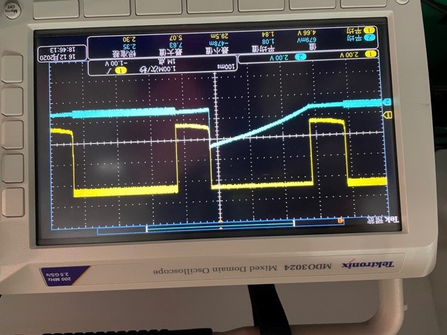
TLC555-Q1 is being used in a turn LED lighting, sometimes(10%) some boards have abnormal output issue as below picture 1, sometimes the boards are good. The control signal RTI+ and RTI-off are floating. The lower curve(blue/white) is the DISCH, the yellow is Vdd. The DISCH is always low on the good boards. 

The yellow curve below is DISCH, the blue curve is OUT, they both are abnormal, they should be low. 

Below yellow curve is Vdd and blue is TRIG, they are normal. The abnormal issue follows with TLC555-Q1, say, if A board is abnormal and B board is normal, we replaced the 555 on A board with the 555 on B board, then A board is normal but B board is abnormal. Could you please help? Thanks. 

  • Hello,

    I think one of your pictures is missing. I don't see the picture for "The yellow curve below is DISCH, the blue curve is OUT, they both are abnormal, they should be low." Can you take waveforms of TRIG, DISCH and OUT on a normal board and an abnormal board so we can compare? Have you made sure that all components on the abnormal boards are soldered correctly and the transistors and diodes are in the correct orientation?

    If the DISC/THRESH node is charging like seen in the first picture, it seems to me like there is a false trigger happening. In the fist picture you say the yellow curve is VDD, so it looks like there is a false trigger happening on powerup? It looks like the timing capacitor charges up to 2/3VDD and returns low right before you cycle VDD. If you powerup VDD one time on an abnormal board, does the output remain low after the initial false trigger? 

  • Hi Jones,

    Thanks for your support. Adding the missed picture first. 

    and adding one more picture to reply your question, the abnormal charging doesn't happen each power up cycle, but another cycle. Below yellow is Vdd, blue is DISCH. 

  • Hello,

    Are the supply bypass capacitors and the control pin bypass capacitor placed close to the device as shown here? 

    False triggers can be a result of noise events seen at the supply or control pin, or there could be something from your trigger circuitry around Q12 that is causing a false trigger. 

  • Hello,

     It sounds like the issue is following the board and not the timer when the units are swapped. Some things to try out for debugging are 

    1. Check the board under a microscope for any cracked solder joints.
      1. If so, try reflowing the solder to make a better connection. 
      2. If there is a cracked solder joint  you can temporarily close the joint with the test probe pressure while pushing down. This will make it appear that section of the board is fine. When you lift the probe up the solder joint can split again. 

    2. Check the board for excess flux. 
      1. Although this is unlikely causing the false trigger, it is always best practice to start off with a clean board.
        1. You can use flux cleaner to remove any excess flux. 
    3. Please do a comparison of voltages between the functioning board and the abnormal board for comparison. 
      1. This may highlight what is causing the issue. 

    4. Lastly, make sure that the components (resistors, capacitors) on the board are all the same. 

    - Chris Featherstone