This thread has been locked.

If you have a related question, please click the "Ask a related question" button in the top right corner. The newly created question will be automatically linked to this question.

DAC3171EVM: problems for DAC; freq, and max voltage

Part Number: DAC3171EVM
Other Parts Discussed in Thread: CDCE62005, DAC3174

Hello, I'm Lee.

I have been using a TSW1400EVM as DAC pattern generator with DAC3171EVM for 1 week.

Now, I have some questions about this system.

First, Does DAC3171EVM need an external clock signal over 500MHz?

In my desk, there only are two function generator 20MHz, 100MHz.

And, should I enter number of Sampling Per Second(SPS) less than clcok freq. ?

I have tested various numbers, such as 1G, 100M, 100k, 1k,and so on,

but there were not any change in output waveform.

(additional) Is there any recommended product with clock signal?

Second, Why my output waveform has less power and different freq. from desired form?

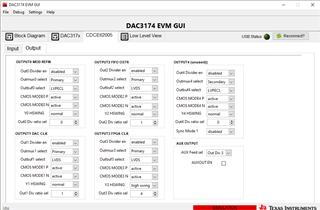
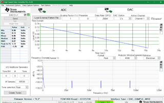
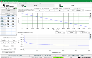
I downloaded Highspeed Data Converter pro and DAC3174GUI in your website,

and I send .reg file that is provided with GUI to DAC3171EVM.

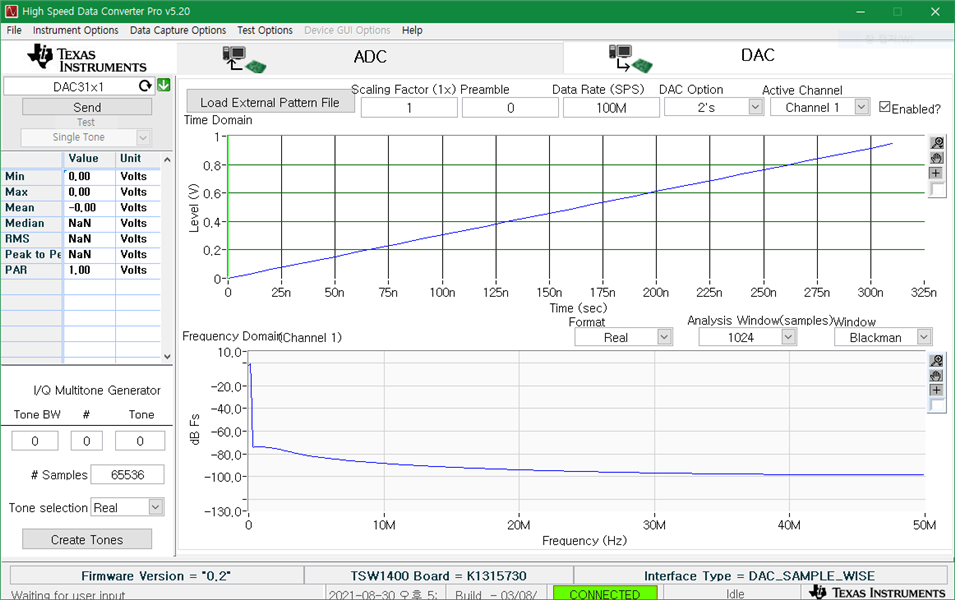
I loaded external pattern file, and this was desired waveform.

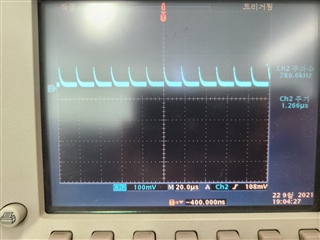
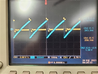
However, the output waveform was this.

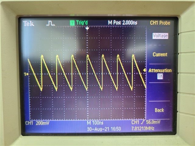
I wished to make a waveform like sawtooth, but the output was reversed and had different freq, max/min voltage.

Why these happen? Is this relative with insufficient clock?

If helpful, I uploaded the external pattern file, dpg1.txt

Please, help me. Thank you.


dpg1.txt
0	0
1000	1000
2000	2000
3000	3000
4000	4000
5000	5000
6000	6000
7000	7000
8000	8000
9000	9000
10000	10000
11000	11000
12000	12000
13000	13000
14000	14000
15000	15000
16000	16000
17000	17000
18000	18000
19000	19000
20000	20000
21000	21000
22000	22000
23000	23000
24000	24000
25000	25000
26000	26000
27000	27000
28000	28000
29000	29000
30000	30000
31000	31000

  • Lee,

    The max clock rate you can use is 500MHz. The board should work fine with your 100MHz generator. Whatever frequency the DAC is using, this should be the sample rate you enter in the HSDC Pro GUI. 

    Make sure the hardware is working properly by using the I/Q tone generator and create a 1MHz output. Send a 100MHz clock to J9 of the DAC3171EVM and see if you can get a valid output. Once you have verified the hardware is working properly, try using your external test file. 

    I think the reg file used by the DAC GUI is incorrect. The clock dividers need to be as shown below. Please try the new config file attached.

    Regards,

    Jim

    new_config_file.cfg

  • Lee,

    After looking at this in more detail, it appears what you are seeing is correct based on the description in the data sheet shown below. Max current output will be with a 0x0000 input data and minimum output current will be with a 0xFFFF input. The DAC does have a complementary option that will allow you to reverse this, which is what I think you are looking for. This is bit 7 of address 0x01.

    Regards,

    Jim

  • Hi, Jim.
    Thank you for helpful advice.
    I used your configuration file, and my output waveform now has less distortion.
    But there are problems about frequency, and Vpp with output signal yet.

    I think my clock signal might cause these problems because its Vpp is only 50mV~100mV.
    The output has 55kHz, 0.3V Vpp but desired is 25kHz and 1V Vpp.
    First of all, is J9(IOUTA2) right output of DAC3171EVM SMA port?
    In my EVM, IOUTA1 port does not have SMA port.

  • Seok,

    The DAC output uses SMA J7 (IOUtA2) by default. If you want a true differential output, you would remove transformer T4 and install SMA J8 (IOUTA1), R36, R40 and R42.

    J9 (EXT_REF_CLK) is used for the clock input.

    Your clock input needs to be at least 100mv as the minimum VINpp is 100mV for the CDCE62005.

    Regards,

    Jim

  • Jim,

    I upgraded my clock signal, 250MHz and 0.15Vpp, and used your new register file, so I tried again but there are same problems.

    First, at DAC3174_v1p2 GUI, there is an option that control TSW1400 CLK, it seems like clk input from DAC3171EVM to TSW1400EVM.

    I changed this value from 1 to 16, and realized it divides the clock by selected value. But I only can see the output signal when the value is 4 ~ 16,

    without 1 ~ 3. I used the clock 250MHz, but I couldn't see the original waveform without clock dividing. The external digital data was single column, length 4096, and 4095 to 0 values. The desired output and one spectated by scope is here. I changed the 0x01 register of DAC, so the output had complemented.

    The CDCE62005 register 3 were C384000

    Why the two-waveform don't match? I attached my external data.

    dpg1024.csv

    Regards,

    Lee

  • Lee,

    I will be looking into this. Please update to v2p0 of the GUI. It is attached.

    Regards,

    Jim

    slac543b_v2p0.zip

  • Lee,

    Use the attached config file, v2p0 of the GUI, and the attached pattern file to get a ramp output. It appears HSDC pro is cascading the imported file so I needed to a 16 bit test pattern for this to work. You do not need to make the board modifications as was mentioned earlier in this post.

    Regards,

    Jim 

    ramp_1.csvdac3174_reg.cfg

  • Jim,

    I tried with your files, and now the output seems like a lamp.

    I think the output is related in # of sample and sampling rate. In ext data I attached, I reduced # of sample 4096 to 256 and then distortion disappeared.

    But Vpp didn't be improved. The desired one is 2Vpp, and the output is only 1.37Vpp.

    There are a bit of register 'DAC gain' and I can't improve it, but only can reduce.

    Why these happen?

    Regards,

    Lee

  • Lee,

    There is no gain option, only attenuation when using register config 10 bits 15:12.

    Please try using a tone generated by the I/Q multitone generator tool in the bottom left of the GUI to verify you can get a 2V output. I think the issue is with the test file you are sending to the DAC.

    In HSDC Pro, I noticed your sample rate shown in the upper right of the GUI is set to 100M. This should always match the DAC sample clock, which I thought was 250MHz.

    The other issue could be the transformer. It may not be charging up to the full value you want before it starts to discharge. One test would be trying a sawtooth instead of a ramp. You may also want to try removing it.

    Regards,

    Jim 

  • Jim,

    I tested the transformer, and found that there was a problem with my SMA port cable. It had took almost 30% of output power.

    Thanks for your kindness. Slight smile

    Then, I saw that there is a gap near 70ns between the output and sync pulse, at the J17 SMA port of TSW1400. And pulse width of sync is 30ns.

    Can I control these delay? I think LVDS delay of DAC GUI means that, but it doesn't operation.

    Also, I want the output can have DC offset 5V, but this doesn't work.

    The electrical condition of these test were 250MHz clk, 256 of # digital data for sawtooth signal of 32640 to 0 single column. 

    Need your help.

    Regards,

    Lee

  • Lee,

    The only way to add this offset would be to use a bias-T after the output. This would allow you to enter any DC level you want.

    The GUI LVDS delay only moves the input data with respect to the sample clock to assist with meeting setup and hold times if needed.  

    See the attached file for instructions on how to delay the output pulse on the TSW1400 SYNC SMA J17. This can only be done in clock cycles. 

    Regards,

    Jim

    Trigger.pptx

  • Jim,

    I will add bias-T as your reply, thanks.

    Now I can see 1MHz ramp signal on output port, and I want to control this frequency.

    I changed the output divider ratio register bits on CDCE62005, and the auxiliary output had changed from 8 to 80.

    (+) in hex, x03 register was from C384000 to C31E000.

    I think, the SMA port J7 of DAC3171EVM(IOUTA2) is not auxiliary output, actually, it is the Output channels 0-4.

    Because, the frequency multiplied by 20, not 10 when I changed x03 register.

    So, I tried to get 100kHz output signal, but there were distortion, such as insufficiency # of samples.

    It seemed like the capture when I replied before. : https://e2e.ti.com/support/data-converters-group/data-converters/f/data-converters-forum/1031695/dac3171evm-problems-for-dac-freq-and-max-voltage/3840975#3840975

    I think that I can solve this problem If I product a new external data with another # of samples.

    But, there would be more easier method to change the frequency of output signal.

    Is there are solutions?

    Regards,

    Lee

  • Hi Lee,

    Jim is out and would be best to answer your question. Please give him a few days to respond.

    Thanks,

    Rob

  • Lee,

    I would suggest leaving all of the clock frequencies as is and provided modified data to the DAC to change the output frequency. HSDC Pro GUI can do this with the multi-tone generator for sinewaves. You should be able to do the same for a ramp but this might require a software program like Matlab to generate this file for you. 

    Regards,

    Jim 

  • Jim,

    I saw that the DAC3171EVM was a current sourcing DAC.

    Should I connect a resistor at the SMA port J7 to spectate voltage?

    I think this output is current so that the output signal has distortion.

    Finally, do TSW1400EVM & DAC3171EVM have flash memory to save configuration files after off the power?

    Should I load config files to EVMs by PC for everytime?

    Regards,

    Lee

  • Lee,

    R37 and R39 (49.9 Ohms) is all you need and these should be installed on the board. If you change these values, you could cause distortion.

    The TSW1400 and DAC boards have no flash memory. The firmware has to be re-loaded every time you cycle power along with the DAC registers settings if they are different than the default reset settings.

    Regards,

    Jim