This thread has been locked.

If you have a related question, please click the "Ask a related question" button in the top right corner. The newly created question will be automatically linked to this question.

DAC34SH84: Multichip multiboard synchronization

Expert 1730 points
Part Number: DAC34SH84
Other Parts Discussed in Thread: DAC34H84, , DAC3484, LMK04828, CDCE62005

Hello,

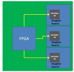
    We plan on having multiple FMC boards each having one DAC34SH84 on a single carrier board with FPGAs. The instantaneous bandwidth of the system is 500MHz. Is it realizable with the DAC34SH84 and the DAC34H84?

2) How do we synchronize the devices on different boards (there is a mention of OSTR for sync) but physically how do we connect them to the different FMC boards. 

3) DACCLK and OSTR are differential signals, do we connect multiple (4 coaxial/SMA cables) to each of these boards?
4) Can we put the clock generation chip on the carrier board and then route them to the DAC ICs through the FMC connectors?

5) Any reference design for interfacing FPGA (Xilinx) to these DACs?

6) The DACs have to generate zero IF I and Q to feed IQ modulators that have single ended inputs. Please advise on suitable circuitry? IQ imbalance correction and LO leakage correction have to be performed as well. Since the ICs already have this feature how will we make use of them if lets say an opamp (transformer is ruled out since the output is zero IF) is used to convert the differential to single ended signals. Do we add some sort of bias-t at the opamp output to introduce the dc for cancelling LO leakage?

Thanks for your help,

  • SM,

    See "Dual Sync Source Mode" in section 2.4 of the attached document.

    Attached is an example IF-to-RF conversion reference design using the DAC34SH84.

    We do not have any example Xilinx reference design we can provide you with.

    Regards,

    Jim

  • SM,

    See "Dual Sync Source Mode" in section 2.4 of the attached document.

    Attached is an example IF-to-RF conversion reference design using the DAC34SH84.

    We do not have any example Xilinx reference design we can provide you with.

    Regards,

    JimDAC348x Synchronization.pdfslau433.pdf7635.TSW30H84EVM-SCH_C.pdf

  • Hello Jim,

              The reference design you mention is for an differential input IQ modulator. We are looking for a modulator with single ended input at zero IF. 

    We have used the DAC3484 and are familiar with the synchronization when the devices are on a  single PCB but what do we do when the devices are on different PCBs?

    2) How do we synchronize the devices on different boards (there is a mention of OSTR for sync) but physically how do we connect them to the different FMC boards. 

    3) DACCLK and OSTR are differential signals, do we connect multiple (4 coaxial/SMA cables) to each of these boards?
    4) Can we put the clock generation chip on the carrier board and then route them to the DAC ICs through the FMC connectors?

    Also, 

    The instantaneous bandwidth of the system is 500MHz. Is it realizable with the DAC34SH84 and the DAC34H84?

    Regards,

    SM.

  • Please send a block diagram as your description is confusing. Are the FPGA's on the same board as the DAC then these boards plug into a mother (carrier) board?

    Most modulators I have dealt with with use I and Q input data. What part are you using that only requires real input data (single-ended)? 

  • The above is the block diagram of our planned implementation.The document speaking about synchronizing multiple DACs speaks about feeding the OSTR signal to the DAC ICs. In our case where the DAC chips are on different daughter boards, how can we send the OSTR signal (from something like the LMK04828). If we place it on the carrier board (green) then we will connectors in between and how well can the boards be synced?

    2) Our modulator also uses I and Q data. They are just not differential (I+/I- and Q+/Q-). The I and Q inputs are single ended.

    3) Can we use the DAC34SH84 to generate 500MHz wide signals? What is the limit (based on FIR filters inside the chip)?

  • SM,

    1. I would suggest using Dual-Sync-Sources Mode and having the clock generator on the same board as the FPGA as shown in Figure 25 of the DAC348x Device Configuration and Synchronization document I sent you. This is the recommended mode of operation for those applications that require precise control of the output timing.

    In order to minimize the skew it is recommended to use the same clock distribution device such as Texas Instruments CDCE62005 or an LMK device to provide the DACCLK and OSTR signals to all the DAC34SH84 devices in the system. Swapping the polarity of the DACCLK outputs with respect to the OSTR ones establishes proper phase relationship. The trace length for DACCLK and OSTR should all be matched to every DAC device.  

     In Dual Sync Sources mode, the FIFO write and read pointers are reset independently. The FIFO write pointer is reset using the LVDS ISTR or SYNC signal, and the FIFO read pointer is reset using the LVPECL OSTR signal. This allows LVPECL OSTR signal to control the phase of the output for either a single chip or multiple chips. Multiple devices can be fully synchronized in this mode.

    In Dual Sync Sources mode, the FIFO read pointers of multiple DAC devices can start at the same location and same exact time instance given that the OSTR and DACCLK signals among all the devices have the same delay.

    The FIFO pointers reset procedure can be done periodically or only once during initialization as the pointers automatically return to the initial position when the FIFO has been filled. To reset the FIFO periodically, it is necessary to have the ISTR, SYNC, and OSTR signals to repeat at multiples of 8 FIFO samples.

    2. I do not see a question for this.

    3. The BW after filtering is 0.8 * data rate. If you are sampling at 1.5Gsps and using 2x interpolation, the data rate will be 750MHz and the BW will be 600MHz. All of the plots in the data sheet go out to 600MHz when using this mode. 

    Regards,

    Jim