This thread has been locked.

If you have a related question, please click the "Ask a related question" button in the top right corner. The newly created question will be automatically linked to this question.

ADS1278-EP: Looking for an ADC

Part Number: ADS1278-EP
Other Parts Discussed in Thread: INA828, , ADS1258-EP, ADS1298R, ADS1258, ADS1278, ADS131M08, ADS131E08, ADS131E08S, ADS1298, REF6125, REF6025

Hi,

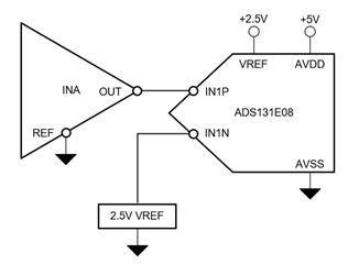
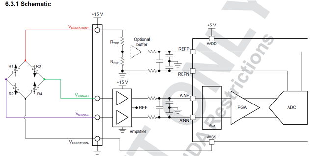
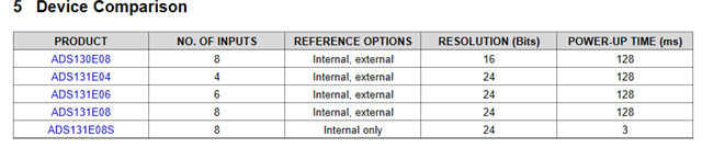
I am looking for an ADC for my application which involves 16 wheatstone bridge loadcells each amplified by an INA828. I am planning to use 2 ADCs, each sampling 8 pseudo differential inputs from the amplifiers at minimally 1k samples per input per second. I am looking at 24 bit ADCs with as high an ENOB and resolution based on the sampling speed I will operate the ADC at to get 1k samples per input ie at least 8ks/s. Currently,  I am looking at these few ADCs, ADS131M08S, ADS1258-EP, ADS1298R or ADS1278-EP, and was wondering if I could get any advice on how to narrow down my choices further or if I have missed out any other options. I would like one that would be in production for a long while yet/have a longevity program since it would be used in a medical product as well.
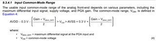
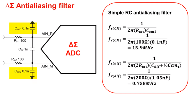
  • Hi Esther,

    How are you planning on supplying the reference voltage to the ADC? Typically bridge measurements use a ratiometric measurement, where the bridge excitation voltage is also used as the ADC reference voltage. Therefore, any variation or drift in the excitation voltage is seen by both the ADC inputs and VREF, and cancels out. Are you going to set up your system this way? If so, what is the excitation voltage for your bridge? This will also require an ADC with differential VREF inputs

    You have a multiplexed ADC (ADS1258) and several simultaneous sampling ADCs in your list. A multiplexed ADC requires a sampling rate of 8 kSPS as you noted (probably longer however, due to filter setting time, etc.), while a simultaneous sampling ADC can convert each input at the same time. Therefore, each channel only needs to sample at 1kSPS for a simultaneous sampling ADC. In the end, you will need a much higher speed multiplexed ADC to measure 8 channels in 1 kSPS.

    The bandwidth of the INA828 is not very high, especially at high gain. I doubt it would have enough bandwidth to drive a part like the ADS1278, which does not have any buffering inside.

    We don't have a device called ADS131M08S, only ADS131M08 or ADS131E08S. I am guessing you meant the ADS131E08, which has been in production for many years. This might be a good device to choose, since it has integrated gain stage that can act as a buffer on the INA output (just set the gain = 1). The ADS131E08 (or ADS131E08S) has differential VREF inputs if you want to choose a ratiometric reference configuration. Finally, with 8x simultaneous ADCs, you can select a data rate of 1 kSPS to get the best noise performance out of the ADC, though the noise will likely be dominated by the INA828 if you are using a high gain. The first ADC sample will be delayed due to the filter, but subsequent conversions in continuous conversion mode will be available at 1kSPS per channel. Or, you can sample at 2kSPS to ensure that data is available within your desired time frame.

    -Bryan

  • Hi Bryan,

    Thanks for your reply. I was thinking to have another reference circuit to supply 2.5V which would be the midpoint of the amplifier's output, but it is not fixed so I can change it to match the input range of the ADC. Or have the amplifier and ADC share the same VREF although I'm not sure what effect that would have on the amplification of the loadcell voltage. My amplifier currently has ground as the VREF.

    I haven't though about using the excitation voltage as VREF though, would it be possible since my bridge excitation voltage is +10V and signal ground ? What would I have to do to get differential VREF inputs? The excitation voltage is on my amplifier PCB right now so if I were to use the same excitation voltage for the ADC, would I have to place them on the same board or can I send the voltage through a wire to the ADC board?

    Are there any benefits of using multiplexed sampling over simultaneous sampling or is simultaneous sampling the way to go nowadays? 

    What would be considered high gain? Currently I have the gain set at 228 to get a little less than 5V on my amplifier output. But again, it is not fixed and I can change it to suit the ADC inputs.

    Yes, I did mean ADS131E08S, sorry about the typo. Is there any differences between continuous conversion mode and only sampling when requested to? Are there any difference between ADS131E08S and ADS1298R or is ADS131E08S the better option overall? Also I see that there is a ADS131E08 and a ADS131E08S. What's the difference between them?

  • Hi Esther,

    Typically you want the common-mode voltage of the INA output at the ADC mid-supply voltage. So if the ADC has AVDD = 5V, then you would want the INA output to be centered at 2.5V. Therefore, the REF pin should be tied to 2.5V, not ground. If you want to supply your ADC with a bipolar supply e.g. +/-2.5V, then the REF pin on the INA should be tied to ground.

    To use a +10V excitation voltage with a 5V ADC, you would need to divide down the 10V excitation or somehow level-shift this voltage into the input range of the ADC. The image below shows how you might design such a circuit. Note that RREF and RTOP need to be precision resistors to make sure the reference is as ratiometric as possible.

    I would hope that the end system would have the INA and the ADC very close to each other to minimize any noise getting picked up by long traces or fly wiring. It sounds like right now you have separate PCBs for the INA and ADC, which is not ideal. If you were to place both of these components on the same board, you can simply divide down the excitation voltage and apply this to the ADC VREF inputs as shown.

    The benefit of using a multiplexed ADC is that they are typically smaller for the same number of channels because they only have 1x ADC inside. However, the challenge with a multiplexed ADC is that the digital filter tends to have to restart each time you change the channel, which can cause delays. A simultaneous sampling ADC can sample all the time, thereby eliminating this conversion latency that results from multiplexing through channels.

    Similarly, continuous conversion mode samples the selected channel repeatedly until you tell the ADC to stop. If you were using single-shot mode, the ADC performs one conversion and then stops. When you tell the ADC to take another conversion, you need to wait for the digital filter to settle before the next conversion is ready. For your application, you would probably want to choose a simultaneous sampling ADC in continuous conversion mode because you have a lot of channels that need to be sampled in a relatively quick period of time (1 kSPS per channel)

    The INA828 specifies a BW of 260kHZ at gain = 100, so this is definitely high gain. Many of our precision ADCs offer gains up to 128, which would also be considered high gain. A gain of 228 V/V is definitely high gain, and would further reduce the BW of the INA828. This is why your ADC input would need to be buffered, because the INA828 does not have enough BW to drive the ADC inputs directly. Again, the ADS131E08 in a gain of 1 is a good choice.

    The ADS131E08 and ADS1298 are similar devices (24-bit, 8-ch simultaneous sampling delta-sigma ADCs). The ADS1298 has several additional features added that make it suitable for ECG or other biopotential measurements. However, those features would not be necessary in this application. But if you are already using the ADS1298 in another application and are very familiar with that device, you could certainly use it for this application. You would just not use the additional ECG features.

    The ADS131E08S is just a fast startup version of the ADS131E08. The E08S does not offer external VREF inputs however, as shown in the table below. So if you want to use a ratiometric reference configuration then you would need to choose the ADS131E08.

    Let me know if you have any additional questions.

    -Bryan

  • Hi Bryan,

    Thanks for the reply. From Table 7.3 in the ADS131E08 datasheet, the VREF can go up to 5V, assuming the AVDD is 5V, which means the maximum differential (in my case pseudo differential) input is 5V. However, based on the equation under 9.3.4.1 Input Common-mode Range as attached, the maximum differential signal can only go up to 4.4V if I were to use AVDD=5V, AVSS=0V and VCM=2.5V 

    Currently, my output from the amplifier ranges from -0.1V to 4.5V with a 0V VREF for the amplifier. If I were to use 2.5V as the VREF for my amplifier, I would have to reduce my amplifier gain to obtain around 2.46 to 4.4V(estimate) as my amplifier output to keep within the differential input range. This would mean I would only be able to use about half of the available codes of the ADC? Could I lower the common-mode voltage to use the full range of codes or is this roughly how I can expect it to be? How would you choose the VREFN and VREFP for the ADC as well? Please correct me if I am wrong, I am not too familiar with how it works!

  • Hi Esther,

    Is the load cell output voltage unipolar or bipolar? If you were measuring weight for example, there can only be a positive output signal because weight is always positive i.e. there is no such thing as negative weight. As a result, you will only ever use the ADC positive code range because your output signal from the bridge is always positive. However, if you were measuring applied force, then that could be potentially be both positive or negative.

    If the output is always positive, then you are only ever going to use the ADC positive code range. And you correctly identified that you will have to change the INA gain to make sure that the INA output voltage is within the ADC common-mode range. However, this is not necessarily a bad thing. You might not actually be able to use all of the ADC code range anyway, depending on how your system is set up. In reality, the main goal is trying to make sure your system is low noise enough to be able to resolve the smallest signal you need to measure. We have some training collateral on this topic: https://training.ti.com/ti-precision-labs-adcs

    I would recommend reviewing the "ADC noise" topics, specifically module 6.4. This video steps through an example resistive bridge calculation. Since you will be using an external amplifier, you might also review module 6.8.

    -Bryan

  • Hi Bryan,

    Thanks for the reply. My output voltage should be unipolar but I sometimes have a slight negative reading due to the zero offset in the loadcell. Thanks for the suggested materials, I will take a look.

  • Hi Esther,

    Yes, a +/- offset voltage is possible, though I would recommend calibrating this initial offset out of the bridge. In some cases the offset voltage can be 10% of the maximum bridge output, resulting in low accuracy.

    Let me know if you have any further questions after reading the content I suggested.

    -Bryan

  • Hi Esther,

    I just wanted to let you know that we just released an application note on bridge measurements: https://www.ti.com/lit/pdf/sbaa532

    This should help support some of the additional questions you may have. I hope all is going well with your design

    -Bryan

  • Hi Bryan,

    Thanks for the link, it looks very helpful.

    I have a few questions actually.

    For ADS131E08, could 5V be used for the VREFP so I can have a max diff input of 2V (with some buffer) with the common mode voltage at 2.5V, or is it advisable to stick to 4V in which case I'll only be able to have 1V for the max differential input? Alternatively, could I use a lower common mode voltage eg 2V? What would be the implications of that? Would the distribution of codes be different in this case eg above 2V produces positive codes, or would they just read below 2.5 as the 'negative' codes.

    Also, I'm currently trying to decide on my input filter. I used the equations below with Rin = 2kohm (estimated. Is there an ideal value for this?) and using fc(dif) = fmod/100 where fmod = fclk/2 and fclk = 2.048MHz

     .

    I got Cdif = 3.9nF and Cm = Cdif/10 = 0.39nF. Would these be appropriate filter values or would using those mentioned in the datasheet (1kohm, Cm = 47pF, Cdif = 0.015uF) be a better choice?

    Incidentally, in this reference design that I found, https://www.ti.com/lit/pdf/tidub80, could I ask what the 0ohm resistors on the SPI pins are for and why those values? Also they placed what I am assuming is a pull-up resistor on the CS pin to DVDD. I'll be using 3.3V for DVDD but I'm using an Arduino to communicate, with level shifters between the SPI pins to convert 3.3V to 5V and vice-versa. I'd just like to confirm that the pull-up on the CS would still work since the DVDD isn't 5V.

  • Hi Esther,

    You can use the largest value of VREF allowed by the device in this application. So if you are selecting the ADS131E08 with AVDD = 5V, then VREF can be up to AVDD, or 5V as well.

    Now, let's say you can tune the output of the INA to be a voltage span of 0.5V to 4.5V, where the INA REF = 0V. Then, you use a precision voltage reference to generate 2.5V and tie this to INxN on each input, so the each INxP input is being measured against 2.5V. You would also set the ADC reference voltage to 2.5V, either by using the pseudo ratiometric reference I discussed previously or by using the same precision reference voltage used to bias INxN. This is all shown in the image below as an example.

    When the INA output is 0.5V (IN1P = 0.5V), the ADC will measure this against IN1N such that VDIFF = IN1P - IN1N = 0.5V - 2.5V = -2V. Using VREF = 2.5V, the ADC output code is approximately -0.8*FS, where FS = full-scale. When the INA output is 4.5V (IN1P = 4.5V), the ADC will measure this against IN1N such that VDIFF = IN1P - IN1N = 4.5V - 2.5V = +2V. Using VREF = 2.5V, the ADC output code is approximately 0.8*FS. This configuration allows you to use most +/-80% of the ADC full-scale range, though you could probably tune the circuit to use more of this range if choose. Just make sure to respect the ADS131E08 common-mode range, as per Equation 4 in the datasheet.

    For more information about choosing the appropriate RC components for the anti-aliasing filter, please review this FAQ: https://e2e.ti.com/support/data-converters-group/data-converters/f/data-converters-forum/955466/faq-delta-sigma-adc-anti-aliasing-filter-component-selection

    The 0ohm resistors on the digital lines are termination resistors. Typically these values would be 30-50ohm, though it appears the architect of this reference design did not feel they were necessary in the final design.

    I am a bit confused by the last question. If you are setting DVDD = 3.3V, why do you need level shifters? Is the IO voltage on the Arduino only 5V? Having a pull-up from CS to DVDD should work as long as the level-shifter is operating properly.

    -Bryan

  • Hi Bryan,

    Thanks for the clarifications. Just to confirm, since the method you suggested uses a pseudo-differential input, do I treat it as a differential signal for the anti-aliasing filter or could I just treat it as a single-ended signal and only filter the input from the amplifier?

  • Hi Esther,

    The reference signal you use to connect to the E08 should already be low noise and have some filtering on the output. Therefore you should be able to use a single-ended RC filter on each INxP input on the E08

    -Bryan

  • Hi Bryan,

    Thanks for the reply. Just to confirm, to calculate the capacitor value for the single-ended RC filter based on the differential mode design guidelines as stated in the link you mentioned, I should used C = 1/(2*pi*R*F) instead of C = 1/(2*pi*2R*F)?

    I'm currently considering REF6125 for the reference signal input as well as VREFP. I was wondering if I can use the circuit in the EVM for REF6025 or should I be changing some of the capacitor/resistor values? Or are there other options I can consider?


  • Hi Esther,

    You are correct about the filter calculation

    The REF6xxx series of voltage references is a good choice because the ADS131E08 VREF inputs are unbuffered. The REF6xxx have an integrated output buffer that keeps the output impedance very low (~50mohm). As far as the VREF circuitry is concerned, what they have shown in the EVM is likely acceptable, though I would always suggest that you read the device datasheet so you can understand why some of the components are necessary and what their component values should be. If you have specific questions about the VREF, you can also reach out to that team via the E2E power management forum.

    -Bryan