This thread has been locked.

If you have a related question, please click the "Ask a related question" button in the top right corner. The newly created question will be automatically linked to this question.

ADC12J2700: JESD204B optical link

Part Number: ADC12J2700
Other Parts Discussed in Thread: TSW14J57EVM, DAC38RF82EVM, DAC38J84EVM, , ADC12DJ5200RF

Hi,

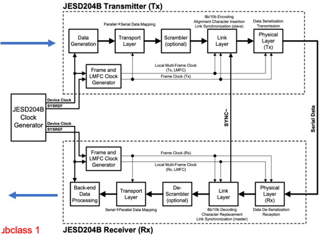
we want to test out a JESD204B link for feed-forwarding of classical data state inside a quantum computer. 

We have a small analog signal coming out of a detector (~10s-100s of mV after RF amplification of these pulses) and we want to send the detection bits on an optical fiber and receive them on the other end to control the paths of a switch and drive their select lines.

We want to use JESD204B link to do that. Would you have an eval board that has the ADC and DACs and the serial mapping, encoding and synching and serialization of the TX JESD204B and of the RX JESD204B? Something that can be quickly setup with our components and that can give us the ability to test out such a link? with GUI and FPGA support etc...?

thanks,

  • Alain,

    Are you interested in the ADC12J2700 ADC as it is in the title of this post? This EVM is available along with a TSW14J57EVM that would be used to capture the data from this JESD204B ADC. We have many other JESD204B/C ADC's to chosen from as well. We have several DAC's available (DAC38J84EVM, DAC38RF82EVM) that use JESD204B and would use the TSW14J57EVM to provide test patterns to the DAC. All boards come with GUI's and are ready to go out of the box.

    It appears you are trying to do a loopback test with an optical setup of some sort, correct?

    Regards,

    Jim  

  • Hi Jim,

    my problem is as follows:

    I have a train of pulses that are the result of some detection events. I need to digitize the presence or absence of a pulse at a particular time and send this information on an optical interconnect. This information is used to set the paths for a switch fabric. I may have several sources of those pulse trains. So I want to map and frame and serialize these onto a JESD204B link.

    I do see that the output bits of each ADC could be mapped, framed, encoded and serialized but I may not need to map the ADC bits but rather map the absence or presence of the pulse (digitized with a comparator with a set threshold?).

    for demonstration, I could use the ADC12J2700 ADC and that will map and frame the ADC bits(+control and tail bits), encode and serialize them. Is that right? does it do this automatically or what bits are mapped can be configured? can the absence or presence of the analog pulse be mapped onto the JESD204B link using that ADC12J2700 device?

    and you say there is a DAC that can recover these bits?

    What is the smallest amplitude and width of the pulse that could be picked up by the ADC? and do I get LVDS (800mVpp) out of the JESD204B TX? I want to drive an optical modulator with it.

    As a 1st step, I think I would need to amplify and digitize the pulses and that will give me the presence or absence of the pulse that I can observe on a scope and compare with the pulse train pre-process. Do you have anything you could suggest me to do that? the output will drive the optical modulator.

    pulse train-->ADC-->comparator/threshold--> pulse present or not-->JESD204B TX-->optical modulator-->optical receiver-->JESD204B RX--> pulse present or not--> drive/set the paths for a switch

    Thanks+Regards,

  • Hi Alain,

    I forwarded this thread to one of our system engineers and he suggested that maybe the ADC12DJ5200RF might be the better ADC of choice since it has 204C and this will eliminate the need for sync (and likely less lanes). However, you will still need clocks, SYSREF and such.

    We have been working on something like this at a high level, but right now we don't have any HW to prove this out. It's still in concept. We do know Samtec has a Firefly board that could hook to the FPGA (and provide MPO cable), but it would need a mating end to the ADC.

    One off the shelf option would be to use a FPGA dev kit, Xilinx, etc. on both ends and use the QSFP cages to send the data over fiber via a pluggable optical module. This will not have low latency, but would enable a plug and play solution without any new HW.

    There may be something offered thru HiTech Global or other COTS vendors. But, we haven’t studied all the options on the market at this moment.

    Regards,

    Rob

  • Hi Rob,

    yes an FPGA dev kit might work but I assume that would involve some development to drive an optical fiber optic module EVB? I am looking for something that I could use readily to drive the fiber optics module EVB. 

    I may start without JESD204B and amplify the pulse trains and try to drive the inputs of the fiber optic EVB. For that I may need some amplifier which I have and a comparator with set threshold that could give me rail to rail output. The second step would be to introduce the JESD204B using ADCs (and DAC on the RX) and the mapping, encoding and serialization (and the opposite on the RX side) functionalities. How can the part numbers that Jim mentioned be used for my application? how can this be made to work plug and play as much as possible?

    can I simply feed my amplified pulse train to the ADC/DAC EVB and insert the link in between the JESD204B TX and RX?

    Thanks,


    Alain

  • Alain,

    Does the attached file look like what you are attempting to test? This was a demo done by one of our former engineers several years back.

    Regards,

    Jim

    JESD204B over Optical.ppt

  • Hi Jim,

    the second bidirectional link is for synch? can the synch be accomplished with this extra link?

    In this demo, the FPGA generates the data and it is sent to the JESD204B RX (DAC) and the DAC is loopback to the ADC of the JESD204B TX that transmit the data back to the FPGA.

    If I want the data to be generated from an analog source (that pulse train I mentioned before) and be recovered on the other end of the link, how would I do this?

    Thanks 

  • I meant ' can the synch be accomplished without that extra link

  • Alain,

    Can you create a block diagram similar to what I sent? This will help us with possibly coming up with a solution for you.

    Regards,

    Jim

  • Hi Jim, I have a train of pulses (top blue arrow) and I want to recover the same train (compare and check error rate. after the TX PHY layer I want to drive a fiber optic module EVB electrically and have an optical loopback on that EVB to the optical RX and use the output of that EVB RX to drive the JESD204B PHY .

  • Alain,

    You should be able to do this using one of our ADC and DAC JESD EVM's. The tricky part is getting the SYNC signal across the link as this is a DC signal. Our demo used a low cost FPGA to code the SYNC using 8b/10b that was then decoded on the other end of the link with another low cost FPGA. All other JESD204 Serdes signals, clock and SYSREF directly feed into an Avago fiber-optical link. This did require a custom board TI built that include the fiber-optical module, power supply, FPGA and FMC connector. Unfortunately, this board is not available but the design files are available if interested.

    If you input the pulse train into the ADC , you should see the pulse train at the output of the DAC. 

    Regards,

    Jim

  • Thanks Jim. Would that board also incorporate the clock generator or is that clock generator on the ADC/DAC JESD EVM? I need the SYNC to pass from JESD TX to RX and the Serdes signals but why do I need to find the clock and SYSREF to the fiber optic modules especially if the clock generator is on the EVM?

    On passing the SYNC, why do you need an FPGA? Wouldn't the SYNC be coded/decoded on the EVM?

  • ...

    why do I need to PASS the clock and SYSREF to the fiber optic modules especially if the clock generator is on the EVM?

  • My mistake. Still getting info from the former engineer who worked on this. The clock was not passed through the fiber but SYSREF was as this is used as a timing reference. The LMK on the receiving side was put into 0-delay mode to generate a phase aligned SYSREF (known phase relative to the SYSREF sent across fiber) as well as the device clocks. So no device clock was actually sent across the fiber since it was generated from SYSREF.

     The TLK3101 was the 8B/10B transceiver used to get the SYNC signal across the fiber. 

  • Hi Jim,

    I am referring to the block diagram I sent out.

    The SYSREF is generated from the clock generator on the EVM. So this is passed to the JESD204B RX through a separate fiber? And the SYNCH is passed on yet another fiber after it goes through the TLK3101 transceiver?

    Can you give me a block diagram/schematic?


    Thanks.

  • Alain,

    That is my understanding. Attached are the schematics of the two boards used along with the ADC and DAC boards and the FPGA pattern generator/data capture card (TSW14J56EVM).

    Regards,

    Jim

    OPTICAL_ADC_DAC-SCH_A.pdfOPTICAL_FPGA-SCH_A.pdf

  • Hi Jim,

    is there a schematic showing connection between the EVM and the fiber optic boards?

    so the channel 10 and 11 on the Fiber optic TX and RX board are used to pass the SYNC and the SYSREF? where is the TLK3101 that handles the SYNC? is that on the TSW14J56EVM? so the other 10 channel is to pass the output of the 8B10B? There is no serialization to a serial optical link like shown in the block diagram above (data serialization)?  

  • Alain,

    I did not work on this project and the engineer that did left our group. I pretty much gave you everything I could. From what I can tell, the TLK3101 was only used to decode the SYNC.  On the Optical ADC/DAC board, the SYNC would go from the DAC and ADC to the on-board TLK3101 and the output for the two SYNC's would each go to CH8 of the Fiber optic modules. There were several SMA's added as spares as far as I can tell. 

    On the Optical FPGA board, the SYNC's had to use the external TLK3101 boards shown in the block diagram as these parts are not on this board. 

    Regards,

    Jim

  • sorry I am a bit confused here...so the JESD TX -->JESD RX goes on one fiber? and you use another fiber to go in the opposite direction? and the SYNCH is going on ch8 of the parallel optics? where does the SYSREF go on a separate fiber as well? what are the other fibers used for?

    in the power point you sent me, where is the SYSREF and SYNC connection? what is the LMK04828EVM for? is that from where SYSREF and device CLK outputs? is that directly connected to one of the optical module input?

  • Allain,

    This is my best guess when looking at the schematics. I could be wrong. I do not have experience with this demo. Since the ADC and DAC boards have their own LMK devices, I am guessing the LMK on the left side of the block diagram is send a reference signal to the ADC and DAC LMK as well as to the LMK on the right side of the block diagram. This will allow all LMK's to be synchronized. The LMK on the right side is providing the device clock and SYSREF to the two TSW14J56EVM boards, which do not have LMK parts. 

    I will see if I can get more info regarding this setup.

    Regards,

    Jim