This thread has been locked.

If you have a related question, please click the "Ask a related question" button in the top right corner. The newly created question will be automatically linked to this question.

ADC12DJ5200RFEVM: ADC12DJ5200RF LINK UP status

Part Number: ADC12DJ5200RFEVM

Hello,

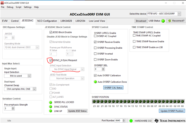
ADCxxDJxx00RF EVM GUI, I can see SERDES PLL Locked LED is green.

This PLL status follows the ADC sampling clock from the external RF signal generator.

But SYNC STATUS and LINK UP LEDs are dark green.

This status means I can't read SerDES output data.

How to debug the point to make ADC LINK UP?

My setup is as follows:

JMODE 31

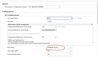
FPGA reference 125 MHz

External Fs 2500 MHz

SerDES rate 8250 MHz

At the FPGA side:

Core clock 124.751 MHz

GTY rx user clock 124.751 MHz 

Sysref 3.906281 MHz

FPGA GTY IBERT measurement 7.997 Gbps

Thanks,

Kiman

  • Hi Kiman,

    Can you please clarify which platform you are using to capture the data from the ADC? 

    JMODE31 is 64b66b mode which means SYNC signal is not used. You can ignore that. 

    Why is core clock 124.751MHz? Should it be 125MHz and the GTY rx user clock should also be 125MHz.

    Regards,

    Neeraj

  • Hi Neeraj,

    I am using the VCK190 Versal board for the JESD204C data readout.

    I added a frequency counter in the FPGA and measured input clocks. It is possibly a very small difference, but I believe that the IBERT line rate is accurate(7.99 Gbps).

    I expected all clocks 125 MHz and 8.25 Gbps line rate from the FPGA side.

    but for unknown reasons clocks and GTY line rate is not matched.

    I am sure an external clock is 125.0 MHz from an RF signal generator.

    Thanks,

    Kiman

  • Hi Neeraj,

    The FPGA frequency count is not accurate, 124.751 MHz seems 125 MHz.

    I attempted using PL clock 125MHz and the frequency counter shows 125.751 MHz.

    If the clock is correct, what is the checkpoint of ADC LINK-UP?

    Thanks,

    Kiman

  • I changed JESD204C parameters and can see LINK UP LED green status.

    - JSYNC_N Sync Request: Enabled

    - SYNC Input selection: NO SYNC Input Signal

    Not sure these changes are good for the JMODE 31.

  • Hi Kiman,

    JMODE31 is 64b66b encoding JESD mode which does not require sync~ signal. In this mode the ADC is always sending data as long it has been programmed and getting proper clock signal. I don't think the above register writes are doing to affect anything in this mode. 

    Can you please check if you are able to lock to ADC data and get the FPGA's PLL to lock?

    Regards,

    Neeraj 

  • Hi Neeraj,

    I can readout 64b/66b raw data using the gt_bridge interface.

    But I can't readout using JESD204C(4.2) output.

    I think the problem is Sync head lock and multi-block lock failure.

    64B66B Sync Header Lock Status: 0

    64B66B Multi-block Lock Status: 0

    SYSREF captured : Ok

    Thanks,

    Kiman

  • Hi Kiman,

    I think the issue is due to mismatch in the ref frequency causing the sync header mismatch errors.

    Regards,

    Neeraj

  • Hi Neeraj,

    Thank you for the update. 

    Versal FPGA does not use JESD204C_PHY IP and used transceiver IP for interface JESD204C IP.

    Can you please see my configuration for the transceiver IP?

    And is meta mode CRC12 for ADC?

    Meta Mode:

    0 = CRC12

    1 = CRC3 (TBD)

    2 = CMD

    3 = FEC

    Thank you.

    Kiman