Other Parts Discussed in Thread: DAC53701, DAC63204, DAC63204EVM
Hello,
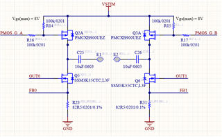
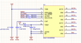
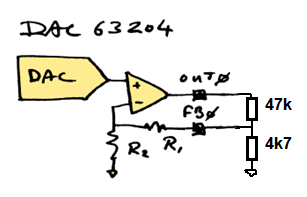
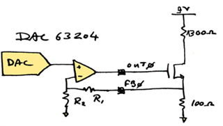
I am using the DAC53004 to control the current in a load with a force-sense configuration with a MOSFET:
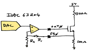
We are doing pulses of 50us/250us, with about 20ms rest in-between.
(The sense resistor is actually 82R, not 100R).
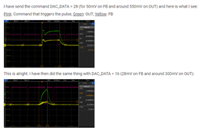
I would like to make the current vary in the load from 5mA to 50uA, which means that the FB voltage varys from 410mV to 4.1mV.
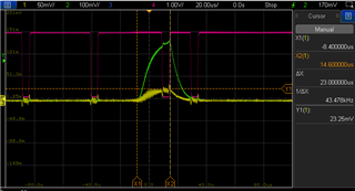
It works well at the beginning, but around 30mV, the setting time becomes longer and longer.
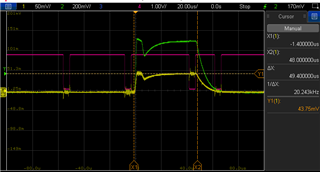
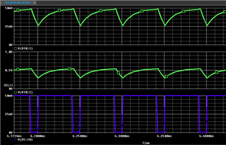
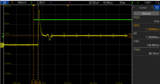
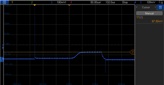
Here you can see a pulse of about 250us (the blue represents the voltage across the 1300R resistor). A 32mV is asked on FB:
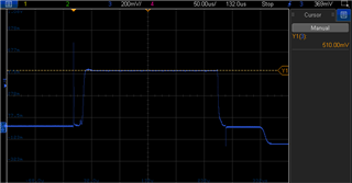
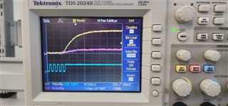
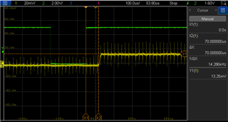
But then you can see that the width of the pulse decreases:
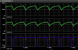
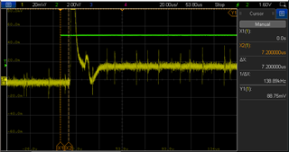
10mV:
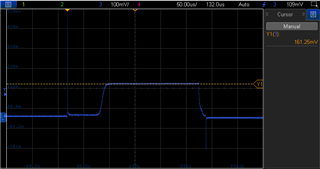
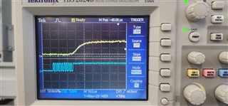
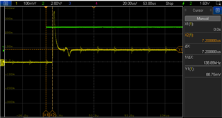
8.2mV:
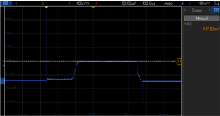
4.2mV:
I can actually see that the OUT voltage of the DAC "struggles" to increase. Is there any limitation at such low voltage?
Best Regards,
Aurélie