This thread has been locked.

If you have a related question, please click the "Ask a related question" button in the top right corner. The newly created question will be automatically linked to this question.

ADS1298ECGFE-PDK: SPI connection with other device

Part Number: ADS1298ECGFE-PDK
Other Parts Discussed in Thread: ADS1298

Hi experts,

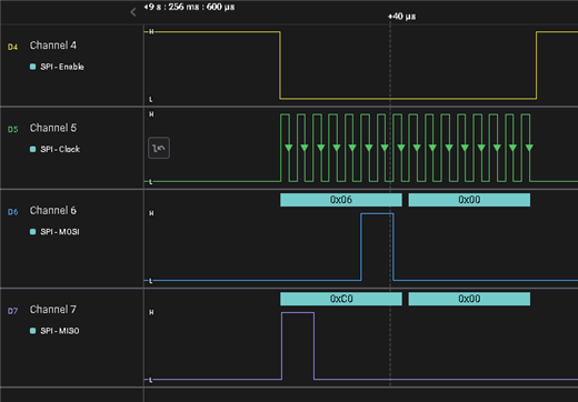
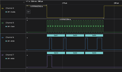
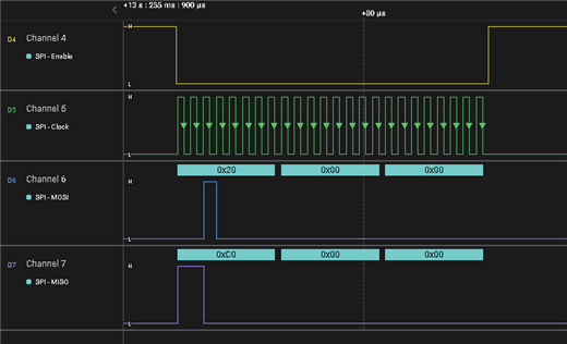
I am trying to connect the ADS1298ECGFE-PDK to one of my custom SPI devices.

To do this, I followed the guidelines I found at this link: https://e2e.ti.com/support/data-converters-group/data-converters/f/data-converters-forum/105352/using-the-ads1298ecgfe-pdk-without-the-mmb0

Despite this, I cannot communicate in SPI with the ADS1298, I receive no response.

Could you please explain to me in detail how to make the connections with my custom device, and how to set the jumpers on the ADS1298ECGFE-PDK.

Thank you for your support.

  • Hi,

    Do you success obtain some of the plots suggested in the post by using the EVM GUI?

    https://e2e.ti.com/support/data-converters-group/data-converters/f/data-converters-forum/1206767/ads1298ecgfe-pdk-differences-between-documentation-calculations-and-software-output

    It's suggested to have a working EVM first before moving on to other host&master(e.g. MCU). Or, do you have two EVMs to work with? Then you can proceed in parallel.

    ------------------------------------------------------------------------------------

    Come back to SPI question-

    1. Did you and How do you verify&validate the host/master's SPI works probably?  Please check that first.

    2. did you power up the ADS1298EVM correctly?

    3. when you say your "custom device", what is that?

    -------------------------------------------------------------------------

    Thanks

  • Bye,
    Regarding the EVM GUI, my colleague will check what you suggested tomorrow.

    Below I respond to the various points regarding the SPI.

    1. Did you and How do you verify&validate the host/master's SPI works probably?  Please check that first.

    The SPI of the master has already been used successfully in the past for SPI communication with other sensors.
    In addition, I am using a protocol analyser (Saleae Logic Pro 8) to check that the communication channel is working properly.
    Via the protocol analyser I can see that the master is able to transmit, but I am not reading anything in response from the ADS1298.

    2. did you power up the ADS1298EVM correctly?

    For the power supply I have connected J4.9 to the respective PIN on MMB0 (3.3V) J4.5 to the respective PIN on MMB0 (GND).
    I have verified that there is 3.3V on TP10.

    3. when you say your "custom device", what is that?

    It is a development board we are using to prototype a medical device.
    This board integrates a SoC with an ARM Cortex-M4 MCU and several communication channels, including SPI.

    Thanks for the support.

  • Hi,

    Do you still use or connect to/via MMB0 board? To communicate with ADS1298 only on the EVM, you don't need the MMB0 board.

    Please disconnect all power and separate the MMB0 board from ADS1298 board.

    Then, resupply the power and make sure the power rails voltages(probed&measured through/via TPs) on the ADS1298 board are the same as what they are when use with an MMB0 board.

    Please use user guide and schematic to compare and verify the voltages.

    Thanks,

    Chien

  • Hi,
    I have completely disconnected the EVM from the MMB0.
    I then powered the EVM via PINs J4.9 (3.3V) and J4.5 (GND).

    I checked with a multimeter that there is 3.3V on TP10.

    Now, what changes do I need to make to the jumpers on the EVM to be able to communicate with my device?
    And what connections should I make between the two devices?

    Thank you for your support.

  • OK.

    Let's do step-by-step.

    1. disconnect ADS1298 board from the host/master, and only supply the power.

    Then take a look of the user guide page 56 -

    2. after supply the power,

    Probe and measure TP7, it should be 5V.

    do you know which digital logic voltage you want to use? e.g. 1.8V or 3.3V, you can select by selecting JP24 jumper position. Then probe at the center pin of JP24, that should be the digital voltage you want. 

    after above, refer to page 37 Table 6 and page 55 to check the voltages. 

    Thanks

  • Hello,
    I have completely disconnected the ADS1298 board from the master
    I only connected the power following page 56
    I have correctly measured 5V on TP7
    I have moved JP24 to position 1-2 to select 1.8V
    I have successfully checked all TPs and verified all power supplies

    How do I proceed now?

  • Great. 

    Now, see if you could refer to user guide page 56, to jump/connect SPI's and other digital signals wires from host/master to J3-x pins; x could be 1,3,11,13,15, 6,8,12.

    You may need to study the datasheet a bit and make decision whether you want to user internal CLK or external CLK? and whether you want to use firmware command to control START or use logic signal to control START, which determine how you want to connect/configure the JP22(START), J3-17 and JP23(CLKSEL).

    Thanks

  • Hi,
    Thank you for your reply.

    I have connected the master's CS to J3.1, CLK to J3.3, MOSI to J3.11, MISO to J3.13.

    I moved JP22 to position 1-2 to use the logic signal to control START, and left JP23 in position 1-2 to use the external clock.
    Is this correct?

    With this configuration, the ADS1298 started to respond.

    When I send the WAKEUP command, I get a 0xC0 response.

    However, trying to read the ID register (via the 0x20 0x00 command) I always get a different response, and not the expected one (which if I am not mistaken should be 0x82).
    Should I change some other hardware setting?

    The firmware settings for the SPI are as follows:
    - CS active low
    - CLOCK 500kHz
    - CPOL 0
    - CPHA 1
    - MSB bit order

    Thank you for your support.

  • Hi,

    Just to confirm, are you now able to sort of interact with the ADS via SPI?

    -------------------------------------------

    If yes, then

    "CLOCK 500kHz",  is this SPI's SCLK?  please make sure it meets the section 7.6 Timing Requirements: Serial Interface -

    "tSCLK SCLK period 50 66.6 ns" depending on your DVDD.

    -----------------------------------------------------------------------------------------

    for "However, trying to read the ID register (via the 0x20 0x00 command) I always get a different response, and not the expected one (which if I am not mistaken should be 0x82).
    Should I change some other hardware setting?"

    Yes, ID register reading is the first thing you want to try.

    Please follow the power-up sequence and RESET procedures properly described in data sheet.

    ADS1298 ID should be 100 10 010, or you can refer to the ADS1298EVM's ID register reading.

    -------------------------------

    Thanks

  • Hi,
    Yes, I seem to be able to communicate in SPI with the ADS.
    The problem is that I'm getting random data that doesn't make sense.

    I will now try to apply your advice.

    By powerup procedure do you mean the flowchart on page 85 of the datasheet?

    Thank you.

  • datasheet page 96 11.1 Power-Up Sequencing or you can probe on a good evm to create/replicate the similar power up timing.

    Thanks

  • Hi,
    Thank you for your reply.

    I followed the power-up procedure on page 96, and the result changed slightly.

    Now the ADS1298 does not send random values, but responds 0xC0 to any command I send.

    Below I attach a few screens of the various commands I send.

    RESET


    SET CONFIG 1


    READ ID

    Could you explain this behaviour to me?

    Thank you for your support.

  • Hi,

    We haven't encountered always returning 0xC0  = b#1100 0000.

    Did you wait long enough after power up and reset?

    11.1 Power-Up Sequencing

    Table 38

    tPOR Wait after power up until reset 2^18 tCLK

    tRST Reset low duration 2 tCLK

    See if you can probe and match your power up sequence similar to Figure 105. Power-Up Timing Diagram

    ----------------------------------------------------

    After above let's go back to focus on making sure you can read the ID register correctly first.

    Can you read the ID register correctly?

    --------------------------------------------

    You can try to compare your SPI waveforms with the other EVM board and/or refer to the following thread for SPI debug&troubleshooting -

    https://e2e.ti.com/support/data-converters-group/data-converters/f/data-converters-forum/772490/faq-ads129x-what-are-the-correct-polarity-and-phase-cpol-cpha-spi-settings/2856911#2856911

    https://e2e.ti.com/support/data-converters-group/data-converters/f/data-converters-forum/775262/faq-ads129x-i-m-having-trouble-communicating-with-my-ads129x-device-via-spi-what-debug-steps-i-should-try/2868427#2868427

    Thanks

  • Hi,
    I should have followed the power-up procedure correctly, as described in section 11.1.
    I correctly applied the delays and adjusted the clock umpulses before and after transmission, but the result does not change.
    Tomorrow I will take the various measurements with the oscilloscope.

    In the meantime, I would like to use the clock provided by the ADS1298's internal oscillator, as described in the datasheet, page 50, section 9.3.2.5.

    To do this, I have to move jumpers JP18 - JP19 and JP23, right?
    I tried moving them following the schematic on page 53 and 56, but the ADS1298 stopped working.
    How should I configure the hardware to use the ADS1298's internal oscillator?

    Thank you for your support.

  • Hi,
    I finally managed to communicate with ADS1298.
    I can now read the ID register correctly.

    But I have another problem: I can only communicate in polling.
    Is there a possibility to communicate in DMA mode as well? If so, how? Do I have to make any hardware modifications?

    P.S.: I am still waiting for guidance on using the ADS1298's internal clock.

    Thanks for your support.

  • Hi,

    Could you please clarify that are your referring to the register reading or the acquired signal reading?

    ---------------------------------------------------------------------------------------

    Would you please clarify what you mean by "polling"? for register reading or the acquired signal reading?

    Have you check the RDATAC or RDATA in datasheet for acquired signal reading?

    And, what you mean be DMA mode? What are you assuming and Are you assuming something that is not listed in datasheet?

    ------------------------------------

    Please refer to datasheet page 50 9.3.2.5 Clock, to see how to set/configure to use the Internal Clock oscillator.

    Thanks