- Ask a related questionWhat is a related question?A related question is a question created from another question. When the related question is created, it will be automatically linked to the original question.
This thread has been locked.
If you have a related question, please click the "Ask a related question" button in the top right corner. The newly created question will be automatically linked to this question.
Hi Experts,
Seeking your assistance on this hardware issue with ADC32J25EVM and TSW14J50EVM data capture. Customer shared his reports below.
I have it all set up and working with the software and the fft being shown. However I am seeing a 10-15db noise on 1 of the channels and cannot understand how this might be the case? is this something you can help with?
I have set up the 2 boards aas per the user guides. Channel 2 has a noise floor of approximately -110dB with channel 1 having a noise floor of -92dB. the fundamental frequency amplitude is consistent in both cases so it can only be noise within one of the channels. The board however looks identical so I and my colleagues cannot understand why this might be.
I have sent the 2 screenshots illustrating the difference (attached)
Regards,
Archie A.


Archie,
There may be an issue with one of the discrete components in the analog front end. Can you take a differential scope probe and monitor the input and see how the two channels compare? For CH1, probe ADC pins 10 & 11 or use R258 and R226. For CH2, probe pins 27 & 26 or use R233 and R234. Also verify the DC common mode voltage is 0.95V on all four pins using a voltmeter.
Regards,
Jim
Hello Jim,
Apology for the delayed update due to recent holiday.
We have looked at the common mode. All four pins read 0.95 V. We have also injected a 30 MHz sine wave and the single-ended and differentials look the same for both ADC channels.
Is there anything else you suggest? We are ordering another ADC32J25EVM board in case it is board related.
Regards,
Archie A.
Archie,
There are several registers that control settings for CHA and CHB separately, such as gain, dither and special mode. Make sure the settings are the same for both CHA and CHB.
Place the part in test pattern mode using the digital ramp mode and verify both CHA and CHB captured results are the same. This would verify there is not an issue with the capture card or the digital outputs of the ADC.
Regards,
Jim
Hi Jim,
Thank you for your response. Cx responded:
We had already had the same ideas and ensured the Channel settings were consistent and working. We also tested all of the test patterns which gave the same result for both CHA and CHB verifying there wasn’t an issue with the card or the outputs.
For your assistance.
Regards,
Archie A.
Hello Jim,
Thank you for your response:
I have received and tested the new ADC32J25EVM board and have seen very indifferent results.
When testing the board last night, CHA and CHB were showing approximately the same noise floor level (~-114 dBFs) as expected/desired. However, upon testing this morning, I have seen two different results. Initially, the noise floor of CHB was showing ~-95 dBFs with CHA having a noise floor of ~-114 dBFs. This was very similar to the first board I tested, however this time CHB had the poor noise floor as compared to CHA in the first board tested. Following this, I reconnected everything and tested the new board again. This time, CHB has a noise floor of ~-65 dBFs.
Unfortunately, I did not take any screenshots or data captures of the first two results, but I have attached the final -65 dBFs result.
Is there anything to suggest why I am seeing the results I am seeing?
I have checked the DC common mode voltage with both channels showing the expected 0.95 V. I will continue to test to see if I see any different results to the current -65 dBFs and will keep you updated.
Look forward to hearing from you.
Regards,
Archie A.


Hi Archie,
The engineer working on this for you is OOO for a few days and will respond to you early next week.
We ordered an EVM for check this ourselves and the EVM is now in the lab, just came in yesterday.
Thanks,
Rob
Hello Rob,
Thank you for the update.
Looking forward to the result by next week.
Regards,
Archie A.
Archie,
Please follow the steps in the attached document. We do not see the issue you are reporting. It is critical you issue an ADC reset before configuring the board.
Regards,
Jim
Hello Jim,
Thank you. Customer have responded:
We have used the ADC reset switch (SW1) on both boards now and both have produced the desired noise floor levels on both channels. For future reference, it might be helpful to add this onto your documentation as I could only see this ‘fix’ for the (ADC32xx and ADC34xx) part of the document.
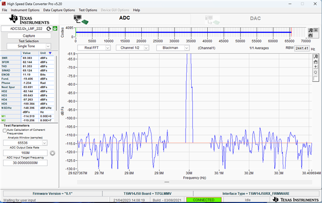
One final question I have is why I am seeing a completely flat line for a small frequency period around the centre frequency band?
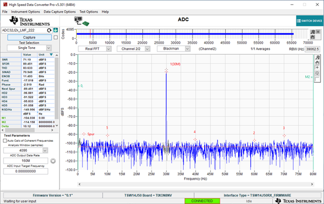
I have attached my FFT response and the FFT response given by your team in the PowerPoint.
Any advice would be greatly appreciated.
Regards,
Archie A.
TI Eval board:
TI Given image:
Archie,
The flat line exists in both plots. You do not see it in the TI plot as the view is not zoomed in. This line is due to the default setting in the GUI to notch out 25 bins on both sides of the fundamental. See attached document for how to adjust this. You can also find out more about this feature in section 3.1.4.1 of the HSDC Pro User's Guide, which I have also attached.
Regards,
Jim