This thread has been locked.

If you have a related question, please click the "Ask a related question" button in the top right corner. The newly created question will be automatically linked to this question.

DAC37J82: No output issue

Part Number: DAC37J82

Hello,

My customer has an issue that the DAC37J82 they designed have no output.

They are using the DAC37J82 with the following conditions.

 - DAC Data Rate input : 245.76Mhz

 - Lane : 4 (LMF = 421)

 - Interpolation : 2

 - DAC Output rate : 491.52Mhz (DAC CLK 491.52Mhz)

 - FPGA JESD CLK : 245.76Mhz

 - JESD Line rate setting value: 2.4576Ghz
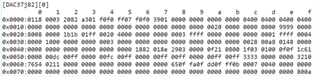
 - Register settings


Here's what they checked:

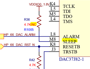
 - TX_Enable = 1 &  ResetB = 1

 - SysRef P/N input (jesd_core clk / 64, 0.96MHz), Alarm 00

 - DAC_SYNC output high (DAC -> FPGA sync signal is high)

 - FPGA -> DAC signal (EYE Diagram)

 - Serdes PLL Locked

 - 4 Lane alignment Alarm OK (0x64/0x65/0x66/0x67 : 0000).

1. What else should they check to fix the DAC37J82 no output issue?

2. They are using only A and D of IOUTx. unused B and C are floating. Could the problem of not connecting the unused IOUT to GND have something to do with the no output?

Thank you.

JH

  • JH,421_CHA_CHD.cfg

    It appears they have the wrong frequency for SYSREF. SYSREF = data rate / (K *N) where N is any whole integer. You cannot get 0.96MHz from this, Try using SYSREF = 1.536MHz or 0.7678MHz. This is assuming they have K set to 10. I have also attached the config file used by our setup using their settings to get an output on CHA and CHD. With CHB and CHC floating, this should not be an issue. Just make sure to power them down by writing 0x26 to address 0x1A.

    Regards,

    Jim

  • Hi Jim,

    The customer modified 0x1A and CHA/CHD path settings based on the registers you shared, but the issue was not cleared.

    For SYSREF, the K value they use is 32. Therefore, it was calculated as follows.

          SYSREF = 2.4576GHz (line rate) / (32(K)*80(N)) = 0.96MHz

    They also verified that there were no errors through the SYSREF Error check of the DAC Alarm Register.

    Therefore, they believe that the previous SYSREF frequency setting had no problems.

    Below is the circuit diagram the customer is using.

      - RX4P/N to RX7P/N are not used

    dac37j82_cropped.pdf

    Please check if there is any problem with the circuit.

    Please advise on what to check additionally to resolve the issue.

    Thank you.

    JH

  • JH,

    They have the sleep input pin tied high. This needs to be tied low.

    Regards,

    Jim

  • Jim

    The pull-up resistor connected to the sleep pin is NC as shown below. According to the datasheet, it's ok to leave it open.

    Regards,

    JH

  • JH,

    Have the customer follow the steps in the attached document to verify the DAC can generate an output tone using just the internal NCO. This will check the clock, power and SPI interface. If they are able to get an output, the issue is probably related to the JESD interface with the FPGA.   

    Regards,

    Jim

    NCO only test.docx